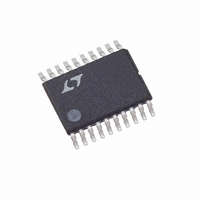
LTC4011CFE#TRPBF Linear Technology, LTC4011CFE#TRPBF Datasheet - Page 8

LTC4011CFE#TRPBF
Manufacturer Part Number
LTC4011CFE#TRPBF
Description
IC BATT CHARGER HIEFF 20TSSOP
Manufacturer
Linear Technology
Datasheet
1.LTC4011CFEPBF.pdf
(26 pages)
Specifications of LTC4011CFE#TRPBF
Function
Charge Management
Battery Type
Nickel Cadmium (NiCd), Nickel Metal-Hydride (NiMH)
Voltage - Supply
4.5 V ~ 34 V
Operating Temperature
0°C ~ 85°C
Mounting Type
Surface Mount
Package / Case
20-TSSOP (0.173", 4.40mm Width) Exposed Pad
Lead Free Status / RoHS Status
Lead free / RoHS Compliant
Available stocks
Company
Part Number
Manufacturer
Quantity
Price
LTC4011
Typical perForMance characTerisTics
pin FuncTions
DCIN (Pin 1): DC Power Sense Input. The LTC4011 senses
voltage on this pin to determine when an external DC
power source is present. This input should be isolated
from V
the Applications Information section for complete details.
Operating voltage range is GND to 34V.
FAULT (Pin 2): Active-Low Fault Indicator Output. The
LTC4011 indicates various battery and internal fault condi-
tions by connecting this pin to GND. Refer to the Operation
and Applications Information sections for further details.
This output is capable of driving an LED and should be
left floating if not used. FAULT is an open-drain output to
GND with an operating voltage range of GND to V
CHRG (Pin 3): Active-Low Charge Indicator Output. The
LTC4011 indicates it is providing charge to the battery by
connecting this pin to GND. Refer to the Operation and
Applications Information sections for further details. This
output is capable of driving an LED and should be left
floating if not used. CHRG is an open-drain output to GND
with an operating voltage range of GND to V
CHEM (Pin 4): Battery Chemistry Selection Input. This
pin should be wired to GND to select NiMH fast charge
termination parameters. If a voltage greater than 2.85V is
applied to this pin, or it is left floating, NiCd parameters
are used. Refer to the Applications Information section for
further details. Operating voltage range is GND to 3.3V.
CC
by a blocking diode or PowerPath FET. Refer to
INTV
DD
Voltage
CC
.
CC
.
GND (Pin 5): Ground. This pin provides a single-point
ground for internal references and other critical analog
circuits.
V
LTC4011 provides 3.3V on this pin to drive an external
thermistor network connected between V
GND. Additional power should not be drawn from this pin
by the host application.
V
thermistor network may be connected to V
temperature-based charge qualification and additional
fast charge termination control. Charging may also be
paused by connecting the V
the Operation and Applications Information sections for
complete details on external thermistor networks and
charge control. If this pin is not used it should be wired
to V
V
nal voltage divider between BAT and V
this pin to monitor the average single-cell voltage of the
battery pack. The LTC4011 uses this information to protect
against catastrophic battery overvoltage and to control
the charging state. Refer to the Applications Information
section for further details on the external divider network.
Operating voltage range is GND to BAT.
TEMP
RT
CELL
(Pin 6): Thermistor Network Termination Output. The
RT
INTV
(Pin 8): Average Single-Cell Voltage Input. An exter-
(Pin 7): Battery Temperature Input. An external
. Operating voltage range is GND to 3.3V.
DD
Short-Circuit Current
TEMP
pin to GND. Refer to
CDIV
TEMP
RT,
is attached to
V
to provide
TEMP
and
4011fb


