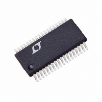
LTC1479CG Linear Technology, LTC1479CG Datasheet - Page 6

LTC1479CG
Manufacturer Part Number
LTC1479CG
Description
IC CTRLR DUAL BATT SYS 36-SSOP
Manufacturer
Linear Technology
Datasheet
1.LTC1479CGPBF.pdf
(24 pages)
Specifications of LTC1479CG
Function
Dual Battery Controller
Battery Type
Lead Acid, Li-Ion, NiCd, NiMH
Voltage - Supply
6 V ~ 28 V
Operating Temperature
0°C ~ 70°C
Mounting Type
Surface Mount
Package / Case
36-SSOP (0.200", 5.30mm Width)
Lead Free Status / RoHS Status
Contains lead / RoHS non-compliant
Available stocks
Company
Part Number
Manufacturer
Quantity
Price
Part Number:
LTC1479CG
Manufacturer:
LT
Quantity:
20 000
Part Number:
LTC1479CG#PBF
Manufacturer:
LINEAR/凌特
Quantity:
20 000
PIN
LTC1479
External Power Supply Pins
DCIN (Pin 1): Supply Input. A 330 resistor should be
put in series with this pin and the external DC power
source. A 0.1 F bypass capacitor should be connected to
this pin as close as possible.
DCDIV (Pin 2): Supply Divider Input. This is a high
impedance comparator input with a 1.215V threshold
(rising edge) and approximately – 35mV hysteresis.
BAT1, BAT2 (Pins 35, 34): Supply Input. These two pins
are the inputs from the two batteries. A 1 F bypass
capacitor should be connected to each pin as close as
possible if there is no larger battery supply capacitor
within 2".
V
the top of the battery resistor ladder to either BAT1 or
BAT2.
BDIV (Pin 33): Battery Divider Input. A high impedance
comparator input with a 1.215V threshold (falling edge)
and approximately 35mV hysteresis.
V
the LTC1479 when in the backup mode of operation. A 1 F
bypass capacitor should be connected to the V
close as possible if there is no larger backup supply
capacitor within 2".
Internal Power Supply Pins
V
with at least a 0.1 F capacitor. The V
used primarily to power internal logic circuitry.
V
3.60V output. Bypass this regulator output with a 2.2 F
tantalum capacitor. This capacitor is required for stability.
V
internal diodes to the DCIN, BAT1 and BAT2 pins and
powers the top of the V
Bypass this pin with a 1 F/35V capacitor.
V
switching regulator is intended only for driving the internal
6
BAT
BKUP
CCP
CC
GG
+
U
(Pin 17): Supply. The V
(Pin 15): Power Supply Output. This is a nominal
(Pin 16): Gate Supply. This high voltage (36.5V)
(Pin 32): Battery Voltage Sense. This pin connects
(Pin 20): Power Supply Output. Bypass this output
(Pin 36): Supply Input. This input supplies power to
FUNCTIONS
U
U
GG
switching regulator inductor.
+
pin is connected via three
CCP
power supply is
BKUP
pin as
micropower gate drive circuitry. Do not load this pin with
any external circuitry. Bypass this pin with a 1 F/50V
capacitor.
SW (Pin 18): Output. This pin drives the “bottom” of the
V
between this pin and the V
GND (Pin 19): Ground. The V
should be returned to this ground which is connected
directly to the source of the N-channel switch in the V
regulator.
Input Power Switches
GA, GB (Pins 4, 6): DCIN Switch Gate Drive. These two
pins drive the gates of the back-to-back N-channel switches
in series with the DCIN input.
SAB (Pin 5): Source Return. The SAB pin is connected to
the sources of SW A and SW B. A small pull-down current
source returns this node to 0V when the switches are
turned off.
GC, GD (Pins 7, 9): BAT1 Switch Gate Drive. These two
pins drive the gates of the back-to-back N-channel
switches in series with the BAT1 input.
SCD (Pin 8): Source Return. The SCD pin is connected to
the sources of SW C and SW D. A small pull-down current
source returns this node to 0V when the switches are
turned off.
GE, GF (Pins 10, 12): BAT2 Switch Gate Drive. These two
pins drive the gates of the back-to-back N-channel
switches in series with the BAT2 input.
SEF (Pin 11): Source Return. The SEF pin is connected to
the sources of SW E and SW F. A small pull-down current
source returns this node to 0V potential when the switches
are turned off.
SENSE
be connected directly to the “top” (switch side) of the low
valued resistor in series with the three input power
selector switch pairs, SW A/B, SW C/D and SW E/F, for
detecting and controlling the inrush current into and out
of the power supply sources and the output capacitor.
GG
switching regulator inductor which is connected
+
(Pin 13): Inrush Current Input. This pin should
+
pin.
GG
and V
+
bypass capacitors
GG


