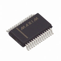
MAX1757EAI+ Maxim Integrated Products, MAX1757EAI+ Datasheet - Page 16

MAX1757EAI+
Manufacturer Part Number
MAX1757EAI+
Description
IC BATTERY CHRG LI+ 28-SSOP
Manufacturer
Maxim Integrated Products
Datasheet
1.MAX1757EAIT.pdf
(17 pages)
Specifications of MAX1757EAI+
Function
Charge Management
Battery Type
Lithium-Ion (Li-Ion)
Voltage - Supply
6 V ~ 14 V
Operating Temperature
-40°C ~ 85°C
Mounting Type
Surface Mount
Package / Case
28-SSOP
Product
Charge Management
Operating Supply Voltage
6 V to 14 V
Supply Current
5 mA
Maximum Operating Temperature
+ 85 C
Minimum Operating Temperature
- 40 C
Charge Safety Timers
Yes
Mounting Style
SMD/SMT
Temperature Monitoring
Yes
Uvlo Start Threshold
2.4 V
Uvlo Stop Threshold
2.6 V
Lead Free Status / RoHS Status
Lead free / RoHS Compliant
Stand-Alone, Switch-Mode
Li+ Battery Charger with Internal 14V Switch
capacitance and ESR rating of the capacitor are impor-
tant for its effectiveness as a filter and to ensure stabili-
ty of the PWM circuit. The minimum output capacitance
for stability is:
where:
The maximum output capacitor ESR required for stabili-
ty is:
where:
The MAX1757 contains four timers: a prequalification
timer, fast-charge timer, full-charge timer, and top-off
timer. Connecting a capacitor from TIMER1 to GND
and TIMER2 to GND sets the timer periods. The
TIMER1 input controls the prequalification, full-charge,
and top-off times while TIMER2 controls the fast-charge
timeout. The typical timeouts for a 1C charge rate are
set to 7.5 minutes for the prequalification timer, 90 min-
utes for the fast-charge timer, 90 minutes for the full-
charge timer, and 45 minutes for the top-off timer by
connecting 1nF capacitors to TIMER1 and TIMER2.
Each timer period is directly proportional to the capaci-
tance at the corresponding pin (see Typical Operating
Characteristics).
Each of the three regulation loops—the input current
limit, the charging current limit, and the charging volt-
age limit—can be compensated separately at the CCS,
CCI, and CCV pins, respectively.
The charge-current loop error amp output is brought
out at CCI. Likewise, the source-current error amplifier
output is brought out at CCS; 0.1µF capacitors to
16
C
V
V
(typically 4.2V per cell).
V
R
R
(100mΩ typ).
REF
BATT
DCIN(MIN)
ESR
CS
OUT
______________________________________________________________________________________
is the current-sense resistor from CS to BATT
is the reference voltage (4.2V).
is the output capacitor ESR.
is the total output capacitance.
is the maximum battery regulation voltage
C
OUT
is the minimum source input voltage.
>
R
ESR
V
V
REF
BATT
<
R
1
x f
CS
+
OSC
V
V
DCIN MIN
x V
REF
Setting the Timers
V
BATT
x R
BATT
(
Compensation
CS
)
ground at CCI and CCS compensate the current loops
in most charger designs. Raising the value of these
capacitors reduces the bandwidth of these loops.
The voltage-regulating loop error amp output is brought
out at CCV. Compensate this loop by connecting a
capacitor in parallel with a series resistor-capacitor (RC)
from CCV to GND. Recommended values are shown in
Figure 1.
A Schottky rectifier with a rating of at least 1.5A must
be connected from LX to PGND.
The MAX1757 uses an internal linear regulator to drop
the input voltage down to 5.4V, which powers the inter-
nal circuitry. The output of the linear regulator is the VL
pin. The internal linear regulator may also be used to
power external circuitry as long as the maximum cur-
rent of the linear regulator is not exceeded.
A 4.7µF bypass capacitor is required at VL to ensure that
the regulator is stable. A 1µF bypass capacitor is also
required between REF and GND to ensure that the inter-
nal 4.2V reference is stable. In both cases, use a low-ESR
ceramic capacitor.
TRANSISTOR COUNT: 5996
Applications Information
VL and REF Bypassing
Chip Information
Diode Selection


