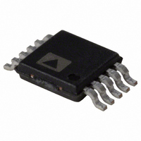
AD8213YRMZ Analog Devices Inc, AD8213YRMZ Datasheet - Page 10

AD8213YRMZ
Manufacturer Part Number
AD8213YRMZ
Description
IC CURRENT MONITOR 0.25% 10MSOP
Manufacturer
Analog Devices Inc
Datasheet
1.AD8213YRMZ-R7.pdf
(16 pages)
Specifications of AD8213YRMZ
Function
Current Monitor
Sensing Method
High-Side
Accuracy
±0.25%
Voltage - Input
-2 ~ 65 V
Operating Temperature
-40°C ~ 125°C
Mounting Type
Surface Mount
Package / Case
10-MSOP, Micro10™, 10-uMAX, 10-uSOP
No. Of Amplifiers
2
Input Offset Voltage
1mV
Gain Db Max
20dB
Bandwidth
500kHz
Cmrr
120dB
Slew Rate
4.5V/µs
Supply Voltage Range
4.5V To 5.5V
Supply Current
2.5mA
Rohs Compliant
Yes
Lead Free Status / RoHS Status
Lead free / RoHS Compliant
Current - Output
-
Available stocks
Company
Part Number
Manufacturer
Quantity
Price
Company:
Part Number:
AD8213YRMZ
Manufacturer:
COMLINEAR
Quantity:
6 225
Part Number:
AD8213YRMZ
Manufacturer:
ADI/亚德诺
Quantity:
20 000
Part Number:
AD8213YRMZ-RL
Manufacturer:
ADI/亚德诺
Quantity:
20 000
AD8213
THEORY OF OPERATION
In typical applications, the AD8213 amplifies a small differential
input voltage generated by the load current flowing through a
shunt resistor. The AD8213 rejects high common-mode
voltages (up to 65 V) and provides a ground referenced, buffered
output that interfaces with an analog-to-digital converter (ADC).
Figure 25 shows a simplified schematic of the AD8213.
The following explanation refers exclusively to Channel 1 of the
AD8213, however, the same explanation applies to Channel 2.
A load current flowing through the external shunt resistor
produces a voltage at the input terminals of the AD8213. The
input terminals are connected to Amplifier A1 by Resistor R1
and Resistor R1
input impedance is held to (V
negligible current flows through Resistor R1
forces the noninverting input to the same potential. Therefore,
the current that flows through Resistor R1
I
IN1
= (I
SHUNT1
OUT2 = (I
(2)
. The inverting terminal, which has very high
× R
SHUNT1
SHUNT2
)/R1
× R
CM
SHUNT2
(1)
) – (I
) × 20
SHUNT
(1)
× R
G = +20
, is equal to
PROPRIETARY
(2)
R2
CIRCUITRY
. Amplifier A1
SHUNT
OFFSET
(1)
), since
CF2
R
I
SHUNT2
SHUNT2
Figure 25. Simplified Schematic
20kΩ
A2
R
R2
OUT2
Rev. A | Page 10 of 16
(2)
(1)
Q2
I
IN2
GND
I
IN1
Q1
R1
R
OUT1
This current (I
output buffer amplifier has a gain of 20 V/V, and offers excellent
accuracy as the internal gain setting resistors are precision
trimmed to within 0.01% matching. The resulting output
voltage is equal to
Prior to the buffer amplifier, a precision-trimmed 20 kΩ resistor
is available to perform low-pass filtering of the input signal
prior to the amplification stage. This means that the noise of the
input signal is not amplified, but rejected, resulting in a more
precise output signal that will directly interface with a converter.
A capacitor from the CF1 pin to GND, will result in a low-pass
filter with a corner frequency of
20kΩ
(1)
R
I
SHUNT1
A1
SHUNT1
PROPRIETARY
V
f
CF1
CIRCUITRY
OUT1
−
OFFSET
3
dB
AD8213
= (I
=
R1
G = +20
2
(2)
π
SHUNT1
IN1
(
20000
) is converted back to a voltage via R
V+
OUT1 = (I
× R
1
)
C
SHUNT1
FILTER
SHUNT1
) × 20
× R
SHUNT1
) × 20
OUT1
. The


