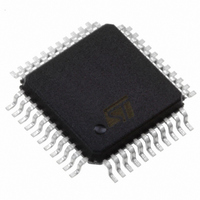
STM86312 STMicroelectronics, STM86312 Datasheet - Page 5

STM86312
Manufacturer Part Number
STM86312
Description
IC DRIVER/CONTROLLER VFD 44PQFP
Manufacturer
STMicroelectronics
Datasheet
1.STM86312.pdf
(24 pages)
Specifications of STM86312
Display Type
Vacuum Fluorescent (VF)
Configuration
16 Segments
Interface
Serial
Digits Or Characters
4 Digits
Voltage - Supply
4.5 V ~ 5.5 V
Operating Temperature
-40°C ~ 85°C
Mounting Type
Surface Mount
Package / Case
44-MQFP, 44-PQFP
Driver Type
VFD Drivers
Maximum Operating Temperature
+ 85 C
Mounting Style
SMD/SMT
Maximum Output Current
25 mA
Minimum Operating Temperature
- 40 C
For Use With
497-5046 - KIT TOOL FOR ST7/UPSD/STR7 MCU
Lead Free Status / RoHS Status
Contains lead / RoHS non-compliant
Current - Supply
-
Lead Free Status / Rohs Status
No
Other names
497-4363
Available stocks
Company
Part Number
Manufacturer
Quantity
Price
STM86312
2.2
Pin description
Table 1. Pin description
10, 11, 12, 13
39, 40, 41, 42
15, 16, 17,
21, 22, 23,
26, 28, 29,
32, 33, 34,
18, 19, 20
35, 36, 37
1, 2, 3, 4
14, 38
24, 25
30, 31
Pin N°
7, 43
27
44
5
6
8
9
SEG12/GRID11 to
GRID1 to GRID6 Grid output pins.
SEG7 to SEG11
SEG16/GRID7
LED1 to LED4
KEY1, KEY2,
SEG1/KS1 to
KEY3, KEY4
SW1, SW2,
SW3, SW4
SEG6/KS6
Symbol
D
OSC
CLK
STB
V
V
V
D
OUT
DD
SS
EE
IN
General-purpose switch inputs.
Output serial data at falling edge of the shift clock, starting
from lower bit. This is N-ch open-drain output pin.
Input serial data at rising edge of the shift clock, starting from
lower bit.
Reads serial data at rising edge, and outputs data at falling
edge.
Initializes serial interface at rising or falling edge to make
STM86312 waiting for reception of command. Data input after
STB has fallen are processed as a command. While command
data are processed, current processing is stopped, and the
serial interface is initialized. While STB is high, CLK is ignored.
Input data to these pins are latched at end of the display cycle.
5V ± 10%.
Segment output pins (Dual function as key source).
Segment output pins.
These pins are selectable for segment or grid driving.
CMOS outputs. +20 mA max.
Connect this pin to system GND.
Pull-down level. V
Connect to an external resistor.
DD
Name and function
- 35V max.
Pin settings
5/24


