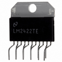
LM2422TE/NOPB National Semiconductor, LM2422TE/NOPB Datasheet - Page 7

LM2422TE/NOPB
Manufacturer Part Number
LM2422TE/NOPB
Description
IC DRIVER MONOLITHIC TO-220-11
Manufacturer
National Semiconductor
Datasheet
1.LM2422TENOPB.pdf
(8 pages)
Specifications of LM2422TE/NOPB
Display Type
CRT
Current - Supply
45mA
Voltage - Supply
100 V ~ 230 V
Mounting Type
Through Hole
Package / Case
TO-220-11 (Bent and Staggered Leads)
Lead Free Status / RoHS Status
Lead free / RoHS Compliant
Operating Temperature
-
Interface
-
Configuration
-
Digits Or Characters
-
Other names
*LM2422TE
*LM2422TE/NOPB
LM2422TE
LM2422TENOPB
LM2422TENOPB
*LM2422TE/NOPB
LM2422TE
LM2422TENOPB
LM2422TENOPB
Available stocks
Company
Part Number
Manufacturer
Quantity
Price
Part Number:
LM2422TE/NOPB
Manufacturer:
NS/国半
Quantity:
20 000
Application Hints
Figure 10 shows the maximum power dissipation of the
LM2422 vs. Frequency when all three channels of the device
are driving into a 10 pF load with a 110V
pixel on, one pixel off. Note that the frequency given in
Figure 10 is half of the pixel frequency. The graph assumes
a 72% active time (device operating at the specified fre-
quency), which is typical in a TV application. The other 28%
of the time the device is assumed to be sitting at the black
level (190V in this case). A TV picture will not have frequency
content over the whole picture exceeding 20 MHz. It is
important to establish the worst case condition under normal
viewing to give a realistic worst-case power dissipation for
the LM2422. One test is a 1 to 30 MHz sine wave sweep
over the active line. This would give a slightly lower power
than taking the average of the power between 1 and 30 MHz.
This average is 23.5 W. A sine wave will dissipate slightly
less power, probably about 21 W or 22 W of power dissipa-
tion. All of this information is critical for the designer to
establish the heat sink requirement for his application. The
designer should note that if the load capacitance is in-
creased the AC component of the total power dissipation will
also increase.
The LM2422 case temperature must be maintained below
110˚C given the maximum power dissipation estimate of
22W. If the maximum expected ambient temperature is 60˚C
and the maximum power dissipation is 22W then a maximum
heat sink thermal resistance can be calculated:
This example assumes a capacitive load of 10 pF and no
resistive load. The designer should note that if the load
capacitance is increased the AC component of the total
power dissipation will also increase.
OPTIMIZING TRANSIENT RESPONSE
Referring to Figure 13, there are three components (R1, R2
and L1) that can be adjusted to optimize the transient re-
sponse of the application circuit. Increasing the values of R1
and R2 will slow the circuit down while decreasing over-
shoot. Increasing the value of L1 will speed up the circuit as
well as increase overshoot. It is very important to use induc-
tors with very high self-resonant frequencies, preferably
above 300 MHz. Ferrite core inductors from J.W. Miller
Magnetics (part # 78FR--K) were used for optimizing the
(Continued)
P-P
alternating one
7
performance of the device in the NSC application board. The
values shown in Figure 13 can be used as a good starting
point for the evaluation of the LM2422. Using a variable
resistor for R1 will simplify finding the value needed for
optimum performance in a given application. Once the opti-
mum value is determined the variable resistor can be re-
placed with a fixed value. Due to arc over considerations it is
recommended that the values shown in Figure 13 not be
changed by a large amount.
Figure 12 shows the typical cathode pulse response with an
output swing of 110V
using the LM1237 pre-amp.
PC BOARD LAYOUT CONSIDERATIONS
For optimum performance, an adequate ground plane, iso-
lation between channels, good supply bypassing and mini-
mizing unwanted feedback are necessary. Also, the length of
the signal traces from the signal inputs to the LM2422 and
from the LM2422 to the CRT cathode should be as short as
possible. The following references are recommended:
Ott, Henry W., “Noise Reduction Techniques in Electronic
Systems”, John Wiley & Sons, New York, 1976.
“Video Amplifier Design for Computer Monitors”, National
Semiconductor Application Note 1013.
Pease, Robert A., “Troubleshooting Analog Circuits”,
Butterworth-Heinemann, 1991.
Because of its high small signal bandwidth, the part may
oscillate in a TV if feedback occurs around the video channel
through the chassis wiring. To prevent this, leads to the video
amplifier input circuit should be shielded, and input circuit
wiring should be spaced as far as possible from output circuit
wiring.
TYPICAL APPLICATION
The typical application for the LM2422 is in HDTV systems
with scan rates as high as 1080i. Full resolution of a 1080i
system requires 30 MHz of bandwidth matching the capabil-
ity of the LM2422. Used in conjunction with an AVP with a
1.2V black level output no buffer transistors are required to
obtain the correct black level at the cathodes. If the AVP has
a black level closer to 2V, then an NPN transistor should be
used to drop the video black level voltage closer to 1.2V.
Some AVPs have black levels at about 2.5V. This level would
require two buffer transistors to drop the black level to the
desired 1.2V. For more information on typical applications or
for demonstration boards please contact your local National
Semiconductor representative.
PP
inside a modified production TV set
www.national.com


