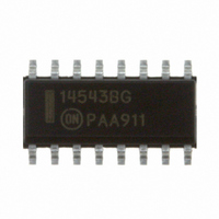
MC14543BDG ON Semiconductor, MC14543BDG Datasheet - Page 5

MC14543BDG
Manufacturer Part Number
MC14543BDG
Description
IC LATCH/DECODER/DRIVER 16SOIC
Manufacturer
ON Semiconductor
Datasheet
1.MC14543BDG.pdf
(8 pages)
Specifications of MC14543BDG
Display Type
LCD
Configuration
7 Segment
Interface
BCD
Current - Supply
10µA
Voltage - Supply
3 V ~ 18 V
Operating Temperature
-55°C ~ 125°C
Mounting Type
Surface Mount
Package / Case
16-SOIC (3.9mm Width)
Product
Decoder / Demultiplexer
Logic Family
MC14
Supply Voltage (max)
18 V
Supply Voltage (min)
3 V
Maximum Operating Temperature
+ 125 C
Minimum Operating Temperature
- 55 C
Mounting Style
SMD/SMT
Power Dissipation
500 mW
Logical Function
Latch/Decoder/Driver
Number Of Elements
1
Polarity
Non-Inverting
Number Of Inputs
4
Number Of Outputs
7
Propagation Delay Time
1650ns
Package Type
SOIC
High Level Output Current
-4.2mA
Low Level Output Current
4.2mA
Operating Supply Voltage (typ)
3.3/5/9/12/15V
Operating Supply Voltage (max)
18V
Operating Supply Voltage (min)
3V
Operating Temp Range
-55C to 125C
Operating Temperature Classification
Military
Mounting
Surface Mount
Pin Count
16
Quiescent Current
20uA
Technology
CMOS
Lead Free Status / RoHS Status
Lead free / RoHS Compliant
Digits Or Characters
-
Lead Free Status / Rohs Status
Lead free / RoHS Compliant
Other names
MC14543BDGOS
Inputs BI and Ph low, and Inputs D and LD high.
f in respect to a system clock.
All outputs connected to respective C
A, B, AND C
ANY OUTPUT
−6.0
−12
−18
−24
Figure 3. Dynamic Power Dissipation
0
−16
Figure 1. Typical Output Source Characteristics
V
20 ns
DD
10%
= 15 Vdc
Signal Waveforms
(V
P
OH
OHmax
50% DUTY CYCLE
− V
−12
DD
= 70 mWdc
90%
V
), SOURCE DEVICE VOLTAGE (Vdc)
2f
1
DD
= 10 Vdc
50%
V
−8.0
SS
20 ns
= 0 Vdc
L
loads.
V
DD
= 5.0 Vdc
V
V
V
V
DD
SS
OH
OL
−4.0
http://onsemi.com
MC14543B
0
5
6.0
24
18
12
0
(a) Inputs D, Ph, and BI low, and Inputs A, B, and LD high.
(b) Inputs D, Ph, and BI low, and Inputs A and B high.
(c) Data DCBA strobed into latches
0
Figure 2. Typical Output Sink Characteristics
C
g
LD
C
g
LD
Figure 4. Dynamic Signal Waveforms
20 ns
t
t
su
PHL
(V
V
90%
DD
OL
4.0
90%
10%
= 5.0 Vdc
− V
50%
SS
10%
t
50%
), SINK DEVICE VOLTAGE (Vdc)
WH
90%
50%
50%
20 ns
V
8.0
t
DD
THL
20 ns
= 10 Vdc
P
t
50%
PLH
OLmax
50%
t
t
h
TLH
10%
V
= 70 mWdc
SS
V
DD
= 0 Vdc
12
= 15 Vdc
V
V
V
V
V
V
V
V
V
V
V
V
DD
SS
OH
OL
DD
SS
DD
SS
OH
OL
DD
SS
16


