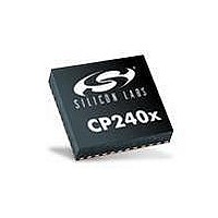
CP2400-GM Silicon Laboratories Inc, CP2400-GM Datasheet - Page 91

CP2400-GM
Manufacturer Part Number
CP2400-GM
Description
IC LCD DRIVER 48QFN
Manufacturer
Silicon Laboratories Inc
Specifications of CP2400-GM
Package / Case
48-QFN
Display Type
LCD
Configuration
128 Segment
Interface
SPI Serial
Current - Supply
620µA
Voltage - Supply
1.8 V ~ 3.6 V
Operating Temperature
-40°C ~ 85°C
Mounting Type
Surface Mount
Data Ram Size
256 B
Interface Type
SPI
Maximum Clock Frequency
25 MHz
Number Of Timers
2
Operating Supply Voltage
1.8 V to 3.6 V
Maximum Operating Temperature
+ 85 C
Mounting Style
SMD/SMT
Minimum Operating Temperature
- 40 C
Lead Free Status / RoHS Status
Lead free / RoHS Compliant
Digits Or Characters
-
Lead Free Status / Rohs Status
Lead free / RoHS Compliant
Other names
336-1855-5
Available stocks
Company
Part Number
Manufacturer
Quantity
Price
Company:
Part Number:
CP2400-GM
Manufacturer:
SIGE
Quantity:
5 000
12.6. Blinking LCD Segments
The LCD driver supports blinking LCD applications such as clock applications where the “colon” separator toggles
on and off once per second. If the LCD is only displaying the hours and minutes, then the device only needs to
wake up once per minute to update the display. The once per second blinking is automatically handled by the
CP2400/1/2/3.
The LCD0BLINK register can be used to enable blinking on any LCD segment connected to the LCD0 or LCD1
segment pin. In static mode, a maximum of 2 segments can blink. In 4-mux mode, a maximum of 8 segments can
blink. The LCD0BLINK mask register targets the same LCD segments as the ULPMEM00 register. If an
LCD0BLINK bit corresponding to an LCD segment is set to 1, then that segment will toggle at the frequency set by
the LCD0TOGR register without any software intervention.
SFR Definition 12.8. LCD0BLINK: LCD0 Blink Mask
Address = 0x80
Name
Reset
Type
7:0
Bit
Bit
LCD0BLINK[7:0]
R/W
7
0
Name
R/W
6
0
LCD0 Blink Mask.
Each bit maps to a specific LCD segment connected to the LCD0 and LCD1 segment
pins. A value of 1 indicates that the segment is blinking. A value of 0 indicates that the
segment is not blinking. This bit to segment mapping is the same as the ULPMEM00
register.
R/W
5
0
Rev. 1.0
R/W
LCD0BLINK[7:0]
4
0
R/W
Function
3
0
R/W
2
0
CP2400/1/2/3
R/W
1
0
R/W
0
0
91


