MC14513BCPG ON Semiconductor, MC14513BCPG Datasheet

IC LATCH/DECODER/DRIVER 18DIP

MC14513BCPG

Manufacturer Part Number
MC14513BCPG
Description
IC LATCH/DECODER/DRIVER 18DIP
Manufacturer
ON Semiconductor
Datasheet

Specifications of MC14513BCPG

Configuration
7 Segment
Interface
BCD
Current - Supply
10µA
Voltage - Supply
3 V ~ 18 V
Operating Temperature
-55°C ~ 125°C
Mounting Type
Through Hole
Package / Case
18-DIP (0.300", 7.62mm)
Lead Free Status / RoHS Status
Lead free / RoHS Compliant
Display Type
-
Digits Or Characters
-
Other names
MC14513BCPGOS

Available stocks

Company
Part Number
Manufacturer
Quantity
Price
Part Number:
MC14513BCPG
Manufacturer:
FREESCALE
Quantity:
101
MC14513B
BCD−To−Seven Segment
Latch/Decoder/Driver
CMOS MSI
(Low−Power Complementary MOS)
constructed with complementary MOS (CMOS) enhancement mode
devices and NPN bipolar output drivers in a single monolithic structure.
The circuit provides the functions of a 4−bit storage latch, an 8421
BCD−to−seven segment decoder, and has output drive capability. Lamp
test (LT), blanking (BI), and latch enable (LE) inputs are used to test the
display, to turn−off or pulse modulate the brightness of the display, and
to store a BCD code, respectively. The Ripple Blanking Input (RBI) and
Ripple Blanking Output (RBO) can be used to suppress either leading
or trailing zeroes. It can be used with seven−segment light emitting
diodes (LED), incandescent, fluorescent, gas discharge, or liquid crystal
readouts either directly or indirectly.
driver, computer/calculator display driver, cockpit display driver, and
various clock, watch, and timer uses.
Features
Stresses exceeding Maximum Ratings may damage the device. Maximum
Ratings are stress ratings only. Functional operation above the Recommended
Operating Conditions is not implied. Extended exposure to stresses above the
Recommended Operating Conditions may affect device reliability.
1. Temperature Derating: Plastic “P and D/DW”
2. P
MAXIMUM RATINGS
© Semiconductor Components Industries, LLC, 2006
June, 2006 − Rev. 6
DC Supply Voltage Range
Input Voltage Range, All Inputs
DC Current Drain per Input Pin
Power Dissipation per Package (Note 1)
Operating Temperature Range
Storage Temperature Range
Maximum Continuous Output Drive
Current (Source) per Output
Maximum Continuous Output Power
(Source) per Output (Note 2)
The MC14513B BCD−to−seven segment latch/decoder/driver is
Applications include instrument (e.g., counter, DVM, etc.) display
Schottky TTL Load to Two HTL Loads Over the Rated Temperature
Range
Low Logic Circuit Power Dissipation
High−Current Sourcing Outputs (Up to 25 mA)
Latch Storage of Binary Input
Blanking Input
Lamp Test Provision
Readout Blanking on all Illegal Input Combinations
Lamp Intensity Modulation Capability
Time Share (Multiplexing) Capability
Adds Ripple Blanking In, Ripple Blanking Out to MC14511B
Supply Voltage Range = 3.0 V to 18 V
Capable of Driving Two Low−Power TTL Loads, One Low−Power
Pb−Free Package is Available*
Packages: – 7.0 mW/_C From 65_C To 125_C
OHmax
= I
OH
Parameter
(V
DD
− V
(Voltages Referenced to V
OH
)
Symbol
P
I
OHmax
OHmax
V
T
V
P
T
DD
stg
I
in
D
A
SS
−0.5 to V
)
−0.5 to +18.0
−55 to +125
−65 to +150
Value
500
10
25
50
DD
+0.5
1
Unit
mW
mW
mA
mA
°C
°C
V
V
the inputs against damage due to high static voltages
or electric fields. However, it is advised that normal
precautions be taken to avoid application of any
voltage higher than maximum rated voltages to this
high−impedance circuit. A destructive high current
mode may occur if V
the range V
damage can occur to the device if V
the outputs are shorted to V
(See Maximum Ratings).
logic voltage level (e.g., either V
MC14513BCP
MC14513BCPG
*For additional information on our Pb−Free strategy
and soldering details, please download the
ON Semiconductor Soldering and Mounting
Techniques Reference Manual, SOLDERRM/D.
This device contains protection circuitry to protect
Due to the sourcing capability of this circuit,
Unused inputs must always be tied to an appropriate
1
Device
ORDERING INFORMATION
18
A
WL
YY
WW
G
1
SS
MARKING DIAGRAM
v (V
http://onsemi.com
= Assembly Location
= Wafer Lot
= Year
= Work Week
= Pb−Free Package
MC14513BCP
AWLYYWWG
in
in
(Pb−Free)
Package
PDIP−18
PDIP−18
and V
or V
Publication Order Number:
out
out
SS
) v V
are not constrained to
and are at a logical 1
SS
DD
or V
CASE 707
DD
P SUFFIX
PDIP−18
20 Units/Rail
20 Units/Rail
.
Shipping
is applied, and
MC14513B/D
DD
).

Related parts for MC14513BCPG

MC14513BCPG Summary of contents

Page 1

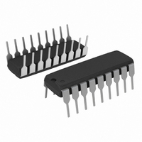
... Pb−Free Package ORDERING INFORMATION Device Package Shipping MC14513BCP PDIP−18 20 Units/Rail MC14513BCPG PDIP−18 20 Units/Rail (Pb−Free) This device contains protection circuitry to protect the inputs against damage due to high static voltages or electric fields. However advised that normal precautions be taken to avoid application of any voltage higher than maximum rated voltages to this high− ...

Page 2

MC14513B PIN ASSIGNMENT RBI DISPLAY TRUTH TABLE Inputs RBI LE BI ...

Page 3

ELECTRICAL CHARACTERISTICS Î Î Î Î Î ...

Page 4

ELECTRICAL CHARACTERISTICS (continued) Î Î Î ...

Page 5

SWITCHING CHARACTERISTICS Î Î Î Î Î ...

Page 6

INPUT C t PLH OUTPUT g t TLH a. Data Propagation Delay: Inputs RBI, D and LE low, and Inputs and LT high INPUT C t PLH OUTPUT RBO t TLH b. Inputs ...

Page 7

CONNECTIONS TO VARIOUS DISPLAY READOUTS LIGHT EMITTING DIODE (LED) READOUT V DD COMMON CATHODE LED V SS INCANDESCENT READOUT GAS DISCHARGE READOUT filament pre−warm resistor is recommended to ...

Page 8

MC14513B LOGIC DIAGRAM RBO RBI 8 http://onsemi.com ...

Page 9

TYPICAL APPLICATIONS FOR RIPPLE BLANKING a − − − − − − − − − − CONNECT TO RBI RBO RBI MC14513B MC14513B ...

Page 10

... Opportunity/Affirmative Action Employer. This literature is subject to all applicable copyright laws and is not for resale in any manner. PUBLICATION ORDERING INFORMATION LITERATURE FULFILLMENT: Literature Distribution Center for ON Semiconductor P.O. Box 5163, Denver, Colorado 80217 USA Phone: 303−675−2175 or 800−344−3860 Toll Free USA/Canada Fax: 303− ...

Related keywords