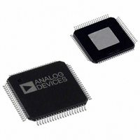
AD8384ASVZ Analog Devices Inc, AD8384ASVZ Datasheet - Page 19

AD8384ASVZ
Manufacturer Part Number
AD8384ASVZ
Description
IC DRIVER LCD 6CH 10BIT 80-TQFP
Manufacturer
Analog Devices Inc
Series
DecDriver™r
Datasheet
1.AD8384ASVZ.pdf
(24 pages)
Specifications of AD8384ASVZ
Display Type
LCD
Interface
3-Wire Serial
Current - Supply
40mA
Voltage - Supply
9 V ~ 18 V
Operating Temperature
0°C ~ 85°C
Mounting Type
Surface Mount
Package / Case
80-TQFP Exposed Pad, 80-eTQFP, 80-HTQFP, 80-VQFP
Lead Free Status / RoHS Status
Lead free / RoHS Compliant
Configuration
-
Digits Or Characters
-
Available stocks
Company
Part Number
Manufacturer
Quantity
Price
Company:
Part Number:
AD8384ASVZ
Manufacturer:
Analog Devices Inc
Quantity:
10 000
PCB DESIGN FOR OPTIMIZED THERMAL
PERFORMANCE
The AD8384’s total maximum power dissipation is partly load
dependent. In a 6-channel 60Hz XGA system running at a
65 MHz clock rate, the total maximum power dissipation is
1.6 W at a 150 pF LCD input capacitance.
At a clock rate of 100 MHz, the total maximum power
dissipation can exceed 2 W, as shown in Table 14, for a black-to-
white video output voltage swing of 4 V and 5 V.
Table 14. Power Dissipation
C
(pF)
150
200
250
300
Although the maximum safe operating junction temperature is
higher, the AD8384 is 100% tested at a junction temperature of
125°C. Consequently, the maximum guaranteed operating
junction temperature is 125°C. To limit the maximum junction
temperature at or below the guaranteed maximum, the package,
in conjunction with the PCB, must effectively conduct heat
away from the junction.
The AD8384 package is designed to provide enhanced thermal
characteristics through the exposed die paddle on the bottom
surface of the package. In order to take full advantage of this
feature, the exposed paddle must be in direct thermal contact
with the PCB, which then serves as a heat sink.
LOAD
P
(W)
1.12
1.12
1.12
1.12
QUIESCENT
P
(W)
0.82
1.01
1.21
1.41
DYNAMIC
V
SWING
= 5 V
P
(W)
1.94
2.13
2.33
2.53
TOTAL
P
(W)
0.71
0.86
1.01
1.17
DYNAMIC
V
SWING
= 4 V
P
(W)
1.83
1.98
2.13
2.29
TOTAL
Rev. 0 | Page 19 of 24
A thermally effective PCB must incorporate two thermal pads
and a thermal via structure. The thermal pad on the top surface
of the PCB provides a solderable contact surface on the top
surface of the PCB. The thermal pad on the bottom PCB layer
provides a surface in direct contact with the ambient. The
thermal via structure provides a thermal path to the inner and
bottom layers of the PCB to remove heat.
THERMAL PAD DESIGN
To minimize thermal performance degradation of production
PCBs, the contact area between the thermal pad and the PCB
should be maximized. Therefore, the size of the thermal pad on
the top PCB layer should match the exposed paddle. The second
thermal pad of the same size should be placed on the bottom
side of the PCB. At least one thermal pad should be in direct
thermal contact with an external plane such as AVCC or GND.
THERMAL VIA STRUCTURE DESIGN
Effective heat transfer from the top to the inner and bottom
layers of the PCB requires thermal vias incorporated into the
thermal pad design. Thermal performance increases
logarithmically with the number of vias.
Near optimum thermal performance of production PCBs is
attained only when tightly spaced thermal vias are placed on the
full extent of the thermal pad.
AD8384


