MAX1365ECM+T Maxim Integrated Products, MAX1365ECM+T Datasheet - Page 2
MAX1365ECM+T
Manufacturer Part Number
MAX1365ECM+T
Description
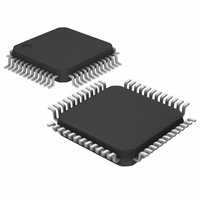
IC PANEL METER 4.5 DIG 48LQFP
Manufacturer
Maxim Integrated Products
Datasheet
1.MAX1367ECM.pdf
(25 pages)
Specifications of MAX1365ECM+T
Display Type
LED
Configuration
7 Segment
Digits Or Characters
A/D 4.5 Digits
Voltage - Supply
2.7 V ~ 5.25 V
Operating Temperature
-40°C ~ 85°C
Mounting Type
Surface Mount
Package / Case
48-LQFP
Lead Free Status / RoHS Status
Lead free / RoHS Compliant
Current - Supply
-
Interface
-


ABSOLUTE MAXIMUM RATINGS
AV
AIN+, AIN-, REF+, REF-.........................V
REG_FORCE, CMP, DAC_VDD, DACVOUT,
EN_BPM, EN_I, REFSELE, DACDATA_SEL, INTREF, RANGE,
NEGV .......................................................-2.6V to (AV
LED_EN....................................................-0.3V to (DV
SET...........................................................-0.3V to (AV
REG_AMP, REG_VDD ...........................................-0.3V to +6.0V
LEDV......................................................................-0.3V to +6.0V
LEDG .....................................................................-0.3V to +0.3V
GND_DAC .............................................................-0.3V to +0.3V
GND_V/I.................................................................-0.3V to +0.3V
Stand-Alone, 4.5-/3.5-Digit Panel Meters
with 4–20mA Output
Stresses beyond those listed under “Absolute Maximum Ratings” may cause permanent damage to the device. These are stress ratings only, and functional
operation of the device at these or any other conditions beyond those indicated in the operational sections of the specifications is not implied. Exposure to
absolute maximum rating conditions for extended periods may affect device reliability.
ELECTRICAL CHARACTERISTICS
(AV
reference), 4-20OUT = 7V, V
noted. All specifications are at T
2
ADC ACCURACY
Noise-Free Resolution
Integral Nonlinearity (Note 1)
Range Change Ratio
Rollover Error
Output Noise
Offset Error (Zero Input Reading)
Gain Error
Offset Drift (Zero Reading Drift)
Gain Drift
INPUT CONVERSION RATE
Update Rate
ANALOG INPUTS (AIN+, AIN-) (bypass to GND with 0.1µF or greater capacitors)
AIN Input Voltage Range (Note 5)
AIN Absolute Input Voltage
Range to GND
Normal-Mode 50Hz and 60Hz
Rejection (Simultaneously)
CONV_IN, 4-20OUT .............................-0.3V to (AV
DPSET1, DPSET2, HOLD, PEAK, DPON,
CS_DAC...............................................-0.3V to (DV
DD,
DD
_______________________________________________________________________________________
DV
= DV
DD ....................................................................
PARAMETER
DD
= DAC_VDD = +2.7V to +5.25V, GND = 0, V
REG_AMP
A
= T
MIN
SYMBOL
= +5.0V, C
INL
NEGV
to T
MAX
to (AV
-0.3V to +6.0V
. Typical values are at T
REF+
MAX1365
MAX1367
2.000V range
200mV range
(V
(V
V
V
(Note 3)
V
RANGE = GND
RANGE = DV
50Hz and 60Hz ±2%
AIN+
AIN+
AIN+
AIN+
AIN+
DD
DD
DD
DD
DD
DD
= 0.1µF, REF- = GND, C
+ 0.3V)
+ 0.3V)
+ 0.3V)
+ 0.3V)
+ 0.3V)
+ 0.3V)
- V
- V
- V
- V
- V
AIN-
AIN-
AIN-
AIN-
AIN-
LEDV
DD
= full scale
= 0 (Note 2)
= 0 (Note 4)
= 0.100V) on 200mV range;
= 0.100V) on 2.0V range
CONDITIONS
= +2.7V to +5.25V, LEDG = 0, V
SEG_ to LEDG.........................................-0.3V to (V
DIG_ to LEDG..........................................-0.3V to (V
REF_DAC .................................................-0.3V to (AV
DIG_ Sink Current .............................................................300mA
DIG_ Source Current...........................................................50mA
SEG_ Sink Current . ............................................................50mA
SEG_ Source Current..........................................................50mA
Maximum Current Input into Any Other Pin . ......................50mA
Continuous Power Dissipation (T
Operating Temperature Range ...........................-40°C to +85°C
Storage Temperature Range .............................-60°C to +150°C
Junction Temperature ......................................................+150°C
Lead Temperature (soldering, 10s) .................................+300°C
48-Pin TQFP (derate 22.7mW/°C above +70°C).....1818.2mW
A
= +25°C, unless otherwise noted.)
NEGV
= 0.1µF. Internal clock mode, unless otherwise
-19,999
-1999
MIN
-0.5
-2.0
-0.2
-2.2
-0
REF+
A
= +70°C)
TYP
10:1
100
- V
0.1
±1
±1
±1
±1
10
5
REF-
+19,999
= 2.048V (external
+1999
MAX
+0.5
+2.0
+0.2
+2.2
+0
LEDV
LEDV
DD
ppm/°C
Counts
Counts
Counts
Counts
UNITS
%FSR
µV
µV/°C
Ratio
+ 0.3V)
+ 0.3V)
+ 0.3V)
dB
Hz
V
V
P-P
Related parts for MAX1365ECM+T
Image
Part Number
Description
Manufacturer
Datasheet
Request
R

Part Number:
Description:
(MAX1365 / MAX1367) Digit Panel Meters
Manufacturer:
Maxim Integrated Products
Datasheet:

Part Number:
Description:
MAX CLIP
Manufacturer:
Aavid Thermalloy
Datasheet:
Part Number:
Description:
MAX7528KCWPMaxim Integrated Products [CMOS Dual 8-Bit Buffered Multiplying DACs]
Manufacturer:
Maxim Integrated Products
Datasheet:
Part Number:
Description:
Single +5V, fully integrated, 1.25Gbps laser diode driver.
Manufacturer:
Maxim Integrated Products
Datasheet:
Part Number:
Description:
Single +5V, fully integrated, 155Mbps laser diode driver.
Manufacturer:
Maxim Integrated Products
Datasheet:
Part Number:
Description:
VRD11/VRD10, K8 Rev F 2/3/4-Phase PWM Controllers with Integrated Dual MOSFET Drivers
Manufacturer:
Maxim Integrated Products
Datasheet:
Part Number:
Description:
Highly Integrated Level 2 SMBus Battery Chargers
Manufacturer:
Maxim Integrated Products
Datasheet:
Part Number:
Description:
Current Monitor and Accumulator with Integrated Sense Resistor; ; Temperature Range: -40°C to +85°C
Manufacturer:
Maxim Integrated Products
Part Number:
Description:
TSSOP 14/A°/RS-485 Transceivers with Integrated 100O/120O Termination Resis
Manufacturer:
Maxim Integrated Products
Part Number:
Description:
TSSOP 14/A°/RS-485 Transceivers with Integrated 100O/120O Termination Resis
Manufacturer:
Maxim Integrated Products
Part Number:
Description:
QFN 16/A°/AC-DC and DC-DC Peak-Current-Mode Converters with Integrated Step
Manufacturer:
Maxim Integrated Products
Part Number:
Description:
TDFN/A/65V, 1A, 600KHZ, SYNCHRONOUS STEP-DOWN REGULATOR WITH INTEGRATED SWI
Manufacturer:
Maxim Integrated Products
Part Number:
Description:
Integrated Temperature Controller f
Manufacturer:
Maxim Integrated Products
Part Number:
Description:
SOT23-6/I°/45MHz to 650MHz, Integrated IF VCOs with Differential Output
Manufacturer:
Maxim Integrated Products
Part Number:
Description:
SOT23-6/I°/45MHz to 650MHz, Integrated IF VCOs with Differential Output
Manufacturer:
Maxim Integrated Products