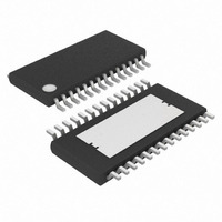
MAX7456EUI+T Maxim Integrated Products, MAX7456EUI+T Datasheet - Page 20

MAX7456EUI+T
Manufacturer Part Number
MAX7456EUI+T
Description
IC DISPLAY 1CH W/EEPROM 28TSSOP
Manufacturer
Maxim Integrated Products
Type
OSD (On-Screen Display) Video Generatorr
Datasheet
1.MAX7456EUI.pdf
(44 pages)
Specifications of MAX7456EUI+T
Applications
Security Systems, Video Routing
Mounting Type
Surface Mount
Package / Case
28-TSSOP Exposed Pad, 28-eTSSOP, 28-HTSSOP
Current - Supply
58mA
Voltage - Supply
4.75 V ~ 5.25 V
Operating Temperature
-40°C ~ 85°C
Interface
SPI Serial
Display Type
OSD
Digits Or Characters
256 Characters
Lead Free Status / RoHS Status
Lead free / RoHS Compliant
Configuration
-
Lead Free Status / Rohs Status
Details
The OSD generator sets each pixel amplitude based on
the content of the character memory and Row
Brightness registers (RB0–RB15).
The OSD insertion mux selects between an OSD pixel
and the input video signal. The OSD image sharpness
is controlled by the OSD Rise and Fall Time bits, and
the OSD Insertion Mux Switching Time bits, found in the
OSD Insertion Mux (OSDM) register. This register con-
trols the trade-off between OSD image sharpness and
crosscolor/crossluma artifacts. Lower time settings pro-
duce sharper pixels, but potentially greater crosscol-
or/crossluma artifacts. The optimum setting depends
on the requirements of the application and, therefore,
can be set by the user.
The MAX7456 includes a video-driver output with a
gain of 2. The driver has a maximum of 2.4V
swing and a 6MHz large signal bandwidth (≤ 0.2dB
attenuation). The driver output is capable of driving two
150Ω standard video loads.
Sag correction is a means of reducing the electrical
and physical size of the output coupling capacitor while
achieving acceptable line-time distortion. Sag correc-
tion refers to the low frequency compensation of the
highpass filter formed by the 150Ω load of a back-ter-
minated coaxial cable and the output coupling capaci-
tor. This breakpoint must be low enough in frequency to
pass the vertical sync interval (< 25Hz for PAL and
< 30Hz for NTSC) to avoid field tilt. Traditionally, the
breakpoint is made < 5Hz, and the coupling capacitor
Single-Channel Monochrome On-Screen
Display with Integrated EEPROM
Figure 13. NVM Structure
20
CMAH [7:0]
______________________________________________________________________________________
On-Screen Display (OSD) Generator
ADDRESS
DECODER
CMAL [5:0]
255
0
Video-Driver Output
.
. .
.
.
.
. .
.
.
.
OSD Insertion Mux
0 . . . . . . . . . . . . . . . . . . . . . . .
CMDI [7:0]
(256 ROWS x 64 BYTES)
64-BYTE SHADOW RAM
Sag Correction
NVM ARRAY
CMDO [7:0]
P-P
output
63
must be very large, typically > 330µF. The MAX7456
reduces the value of this capacitor, replacing it with two
smaller capacitors (C
reducing the size and cost of the coupling capacitors
while achieving acceptable line-time distortion (Table 2).
Connect SAG to VOUT if not used.
The SPI-compatible serial interface programs the oper-
ating modes and OSD data. Read capability permits
write verification and reading the Status (STAT), Display
Memory Data Out (DMDO), and Character Memory
Data Out (CMDO) registers.
The MAX7456 supports interface clocks (SCLK) up to
10MHz. Figure 15 illustrates writing data and Figure 16
illustrates reading data from the MAX7456. Bring CS
low to enable the serial interface. Data is clocked in at
SDIN on the rising edge of SCLK. When CS transitions
high, data is latched into the input register. If CS goes
high in the middle of a transmission, the sequence is
aborted (i.e., data does not get written into the regis-
ters). After CS is brought low, the device waits for the
first byte to be clocked into SDIN to identify the type of
data transfer being executed.
The SPI commands are 16 bits long with the 8 most sig-
nificant bits (MSBs) representing the register address
and the 8 least significant bits (LSBs) representing the
data (Figures 15 and 16). There are two exceptions to
this arrangement:
1) Auto-increment write mode used for display memory
2) Reading character data from the display memory,
Table 2. SAG-Correction Capacitor Values
access is a single 8-bit operation (Figure 21). When
performing the auto-increment write for the display
memory, the 8-bit address is internally generated,
and only 8-bit data is required at the serial interface.
when in 16-bit operation mode, is a 24-bit operation
(8-bit address plus 16-bit data). See Figure 20.
C
OUT
470
100
100
47
22
10
(µF)
C
SAG
22
47
22
10
—
—
OUT
(µF)
Read and Write Operations
and C
LINE-TIME DISTORTION
SAG
Serial Interface
), substantially
(% typ)
0.2
0.4
0.3
0.3
0.4
0.6


