AD8380JS Analog Devices Inc, AD8380JS Datasheet - Page 2
AD8380JS
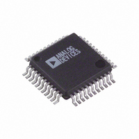
Manufacturer Part Number
AD8380JS
Description
IC LCD DRIVER 6CH 44-MQFP
Manufacturer
Analog Devices Inc
Series
DecDriver™r
Datasheet
1.AD8380JS.pdf
(16 pages)
Specifications of AD8380JS
Rohs Status
RoHS non-compliant
Display Type
LCD
Interface
Parallel
Current - Supply
500µA
Voltage - Supply
9 V ~ 24 V
Operating Temperature
0°C ~ 85°C
Mounting Type
Surface Mount
Package / Case
44-MQFP, 44-PQFP
Configuration
-
Digits Or Characters
-
Available stocks
Company
Part Number
Manufacturer
Quantity
Price
Company:

Part Number:
AD8380JS
Manufacturer:
HRS
Quantity:
1 600


Model
VIDEO DC PERFORMANCE
REFERENCE INPUTS
RESOLUTION
DIGITAL INPUT CHARACTERISTICS
VIDEO OUTPUT CHARACTERISTICS
VIDEO OUTPUT DYNAMIC PERFORMANCE
POWER SUPPLY
OPERATING TEMPERATURE RANGE
NOTES
1
2
3
4
5
6
7
Specifications subject to change without notice.
AD8380–SPECIFICATIONS
See Figure 1 for valid ranges of VMID.
VREFHI Input Current = (VREFHI – VREFLO)/(VREFHI Input Resistance) = 2.5 V/3.3 kΩ.
Delay time from 50% of falling CLK edge to 50% of output change. Measurement is made for both states of INV.
For best settling time results, use minimum series output resistance, R
An output channel is selected, and glitch is monitored as CLK is driven. STSQ and XFR are set to logic low.
Input data is loaded such that any five output channels change by VFS (i.e., 5 V), and the sixth unselected channel is monitored. Measurement is made for both states of INV.
For definitions of VDE and VCME, see the Transfer Function section. Scale factor error is expressed as percentage of VFS.
VDE
VCME
Scale Factor Error
Offset Error
VMID Range
VMID Bias Current
VFS Range
VREFHI
VREFLO
VREFHI Input Resistance
VREFLO Bias Current
VREFHI Input Current
Coding
Input Data Update Rate
C
I
V
V
V
Output Voltage Swing
CLK to VID Delay
Output Current
Data Switching Slew Rate
Invert Switching Slew Rate
Data Switching Settling Time to 1%
Data Switching Settling Time to 0.25%
Invert Switching Settling Time to 1%
Invert Switching Settling Time to 0.25%
CLK Feedthrough
All-Hostile Crosstalk
Supply Rejection (VDE)
DVCC, Operating Range
DVCC, Quiescent Current
AVCC, Operating Range
Total AVCC Quiescent Current
STBY AVCC Current
STBY DVCC Current
IN
IH
IL
TH
IN
Clock to Data Setup Times: t
Clock to STSQ Setup Times: t
Clock to XFR Setup Times: t
Maximum CLK Rise and Fall Time, t
Clock to A[0:2] Hold Times: t
Clock to Data Hold Times: t
Clock to STSQ Hold Times: t
Clock to XFR Hold Times: t
Clock to A[0:2] Setup Times: t
Amplitude
Glitch Duration
2
6
4
7
3
1
2
6
1
5
4
9
3
8
5
5
7
Conditions
T
DAC Code = 450 to 800
DAC Code = 450 to 800
VFS = 2 × (VREFHI–VREFLO)
VFS = 5 V
Binary
Threshold Voltage
AVCC – V
50% of VIDx
T
C
+V
STBY = H
STBY = H
DAC Code = 0 to 1023
DAC Code = 0 to 1023
to VREFLO
MIN
MIN
L
S
= 150 pF, R
= 15 V ± 1 V
to T
to T
(@ 25 C, AVCC = 15 V, DVCC = 3.3 V, T
otherwise noted)
S
of 25 Ω.
MAX
MAX
OH
, V
, V
S
OL
O
= 25 Ω
= 5 V Step,
– AVEE
Min
–7.5
–3.5
–0.25
–7
6
1
VREFLO +0.5
VMID – 0.5
10
1
1
1
4
4
4
4
4
1
2.0
13.5
30
3
9
0
MIN
= 0 C, T
Typ
7
3
5
AVCC – 2.5
VREFHI – 2.5 VREFHI – 0.5
0.2
75
0.6
270
625
26
30
2
95
40
22
33
+1
+0.5
+1
3.3
750
1.4
1.1
15.5
35
85
1
0.5
0.1
MAX
= 85 C, unless
Max
+7.5
+3.5
+0.25
+7
7.5
6
AVCC
3
0.8
1.3
17.5
32
65
40
100
5
5.5
35
24
44
5
5
85
Unit
mV
mV
%
mV
V
µA
V
V
V
kΩ
µA
µA
Bits
Ms/s
ns
ns
ns
ns
ns
ns
ns
ns
ns
pF
µA
V
V
V
V
ns
mA
V/µs
V/µs
ns
ns
ns
ns
mV p-p
mV p-p
ns
mV/V
V
mA
V
mA
mA
mA
°C
Related parts for AD8380JS
Image
Part Number
Description
Manufacturer
Datasheet
Request
R

Part Number:
Description:
±1.7g Dual-Axis IMEMS Accelerometer Evaluation Board
Manufacturer:
Analog Devices Inc
Datasheet:

Part Number:
Description:
Inertial Sensor Evaluation System
Manufacturer:
Analog Devices Inc
Datasheet:
Part Number:
Description:
Manufacturer:
Analog Devices Inc
Datasheet:
Part Number:
Description:
Manufacturer:
Analog Devices Inc
Datasheet:
Part Number:
Description:
Manufacturer:
Analog Devices Inc
Datasheet:
Part Number:
Description:
Manufacturer:
Analog Devices Inc
Datasheet:
Part Number:
Description:
Manufacturer:
Analog Devices Inc
Datasheet:
Part Number:
Description:
Manufacturer:
Analog Devices Inc
Datasheet:
Part Number:
Description:
Manufacturer:
Analog Devices Inc
Datasheet:
Part Number:
Description:
Manufacturer:
Analog Devices Inc
Datasheet:
Part Number:
Description:
Manufacturer:
Analog Devices Inc
Datasheet:
Part Number:
Description:
Manufacturer:
Analog Devices Inc
Datasheet:
Part Number:
Description:
Manufacturer:
Analog Devices Inc
Datasheet: