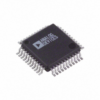
AD8380JSZ Analog Devices Inc, AD8380JSZ Datasheet - Page 3

AD8380JSZ
Manufacturer Part Number
AD8380JSZ
Description
IC DECDRIVER LCD 6CH-OUT 44-MQFP
Manufacturer
Analog Devices Inc
Series
DecDriver™r
Datasheet
1.AD8380JS.pdf
(16 pages)
Specifications of AD8380JSZ
Display Type
LCD
Interface
Parallel
Current - Supply
500µA
Voltage - Supply
9 V ~ 24 V
Operating Temperature
0°C ~ 85°C
Mounting Type
Surface Mount
Package / Case
44-MQFP, 44-PQFP
Lead Free Status / RoHS Status
Lead free / RoHS Compliant
Configuration
-
Digits Or Characters
-
Pin No.
1
2–11
12
13
14
15, 16
17, 20, 22, 24,
26, 28, 30, 32,
34, 37, 38
18
19
21
23, 25, 27, 29,
31, 33
36, 35
39–41
42
43
44
CHANNEL SELECTION FUNCTIONALITY
There are two channel selection modes, addressed channel
loading, (in which the user directly controls which DAC is
loaded), and internally sequenced loading (in which the user
controls the direction and clock phase in which the loading
proceeds).
ADDRESSED CHANNEL LOADING:
When channel address (A0, A1, A2) = 000 through 101, the
video data is loaded into Channels 0 through 5. (STSQ/CS
functions as “Chip Selection” this case.)
INTERNALLY SEQUENCED LOADING:
When channel address = 111 the video data is loaded in a
sequence determined internally. The sequencing is initiated by
a pulse applied to STSQ/CS input. The count proceeds from
0 to 5 if R/L is LOW or from 5 to 0 if R/L is HIGH.
DAC TRANSFER FUNCTION
where VFS = 2 × (VREFHI – VREFLO)
V
V
OUT
OUT
= VMID + VFS × (1 – N/1023); if INV is HIGH,
= VMID – VFS × (1 – N/1023); if INV is LOW
Mnemonic
NC
DB[0:9]
E/O
R/L
INV
DVEE, DVCC
AVCCxxx, AVEExxx Analog Supplies. Nominally 15 V and 0 V, respectively.
STBY
BYP
VMID
VID5–VID0
VREFHI, VREFLO Voltage between these pins sets DAC full-scale range. An external reference must be applied
A[0:2]
STSQ/CS
XFR
CLK
Video Data Inputs. DB9 is the MSB.
Stand By. When high, all digital and analog circuits are “debiased” and the power dissipation
An external capacitor connected from here to V
Externally supplied voltage applied here sets the midpoint reference for the video output.
Analog Video Outputs.
3-bit channel address for addressable loading of the digital input latches.
STSQ to start internal sequencing or Chip Select to enable addressable channel addressing.
If XFR = HIGH at the rising edge of CLK, data is transferred to the DACs on the next falling
Description
No Connect.
Even/Odd data select, input latches are loaded at the falling edge of CLK if E/O is low or
rising edge if E/O is high.
Determines starting point of internally generated channel-loading sequence.
R/L Low (when address = 111) loads from Channel 0 up to Channel 5.
When high, analog video outputs are above the VMID setpoint. See Figure 3.
Digital Supplies. Nominally 3.3 V and 0 V, respectively.
drops to a minimum.
and should be common to all devices to ensure best tracking.
See functional description. Used in conjunction with A[0:2].
edge of CLK. See Figures 4, 6, 7, and 8.
Master Clock Input.
PIN FUNCTION DESCRIPTIONS
MAXIMUM OUTPUT VOLTAGE
The maximum output signal swing is constrained by the output
voltage compliance of the DACs and the output dynamic range
of the output amplifiers. The minimum voltage allowed at the
outputs of the DACs is about 6 V. This constrains the minimum
value of VMID to be 6 V. The output amplifiers will swing and
settle cleanly, as described on the specification page, for output
voltages within 1.5 V from each supply voltage rail.
For a given value of V
video output voltages defines the maximum usable full-scale
voltage. For example, if VMID is less than AVCC/2, the maxi-
mum value of VFS is (VMID – 1.5 V). If VMID is greater than
AVCC/2, the maximum useful VFS is (AVCC – 1.5 – VMID).
Figure 1 graphically describes these limiting factors.
4.5
6
EE
6
will help to ensure rapid DAC settling time.
MID
, the voltage required to saturate the
VMID – Volts
AD8380
7.5


