STLVDS385BTR STMicroelectronics, STLVDS385BTR Datasheet - Page 8
STLVDS385BTR
Manufacturer Part Number
STLVDS385BTR
Description
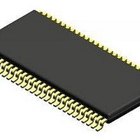
IC FLAT PANEL DISPLY DVR 56TSSOP
Manufacturer
STMicroelectronics
Type
LVDSr
Datasheet
1.STLVDS385BTR.pdf
(19 pages)
Specifications of STLVDS385BTR
Display Type
FPD
Voltage - Supply
3 V ~ 3.6 V
Operating Temperature
0°C ~ 70°C
Mounting Type
Surface Mount
Package / Case
56-TSSOP
Number Of Drivers
4
Number Of Receivers
28
Data Rate
595 Mbps
Operating Supply Voltage
3.3 V
Maximum Power Dissipation
130 mW
Maximum Operating Temperature
+ 70 C
Minimum Operating Temperature
- 10 C
Mounting Style
SMD/SMT
Supply Voltage (max)
3.6 V
Supply Voltage (min)
3 V
Lead Free Status / RoHS Status
Contains lead / RoHS non-compliant
Current - Supply
-
Interface
-
Configuration
-
Digits Or Characters
-
Lead Free Status / Rohs Status
Details
Other names
497-2150-2
Available stocks
Company
Part Number
Manufacturer
Quantity
Price

Part Number:
STLVDS385BTR
Manufacturer:
ST
Quantity:
20 000


Table 10.
Note:
8/19
Symbol
t
t
PLLS
PDD
1
2
3
4
5
6
7
8
Transmitter phase lock loop set
Transmitter power down delay
Transmitter switching characteristics (continued) (V
otherwise noted. Typical values are referred to T
negative. Voltages are referenced to ground unless otherwise specified (except V
Δ
V
The minimum and maximum limits are based on statistical analysis of the device
performance over process, voltage, and temperature range. This parameter is functionality
tested only on automatic test equipment (ATE).
The limits are based on bench characterization of the device’s jitter response over the power
supply voltage range. Output clock jitter is measured with a cycle-to-cycle jitter of ± 3 ns
applied to the input clock signal while data inputs are switching. A jitter event of 3 ns,
represents worse case jump in the clock edge from most graphics controller VGA chips
currently available.
The worst case test pattern produces a maximum toggling of digital circuits, LVDS I/O and
CMOS/TTL I/O.
The 16 grayscale test pattern tests device power consumption for a “typical” LCD display
pattern. The test pattern approximates signal switching needed to produce groups of 16
vertical stripes across the display.
Figure
Recommended pin to signal mapping. Customer may choose to define differently.
Current into device pins is defined as positive. Current out of device pins is defined as
V
OS
OD
previously referred as V
).
2,
Figure 3
Parameter
show a falling edge data strobe (TxCLK IN/RxCLK OUT).
(Figure
(Figure
CM
.
11)
9)
Test conditions
A
= 25 °C)
CC
= 3.3 V, T
Min.
J
Typ.
= -10 to 70 °C unless
Max.
100
10
OD
and
Unit
ms
ns
Related parts for STLVDS385BTR
Image
Part Number
Description
Manufacturer
Datasheet
Request
R

Part Number:
Description:
STMicroelectronics [RIPPLE-CARRY BINARY COUNTER/DIVIDERS]
Manufacturer:
STMicroelectronics
Datasheet:
Part Number:
Description:
STMicroelectronics [LIQUID-CRYSTAL DISPLAY DRIVERS]
Manufacturer:
STMicroelectronics
Datasheet:

Part Number:
Description:
BOARD EVAL FOR MEMS SENSORS
Manufacturer:
STMicroelectronics
Datasheet:
Part Number:
Description:
NPN TRANSISTOR POWER MODULE
Manufacturer:
STMicroelectronics
Datasheet:
Part Number:
Description:
TURBOSWITCH ULTRA-FAST HIGH VOLTAGE DIODE
Manufacturer:
STMicroelectronics
Datasheet:
Part Number:
Description:
Manufacturer:
STMicroelectronics
Datasheet:
Part Number:
Description:
DIODE / SCR MODULE
Manufacturer:
STMicroelectronics
Datasheet:
Part Number:
Description:
DIODE / SCR MODULE
Manufacturer:
STMicroelectronics
Datasheet:
Part Number:
Description:
Search -----> STE16N100
Manufacturer:
STMicroelectronics
Datasheet:
Part Number:
Description:
Search ---> STE53NA50
Manufacturer:
STMicroelectronics
Datasheet:
Part Number:
Description:
NPN Transistor Power Module
Manufacturer:
STMicroelectronics
Datasheet:
Part Number:
Description:
DIODE / SCR MODULE
Manufacturer:
STMicroelectronics
Datasheet: