LM2463TA/NOPB National Semiconductor, LM2463TA/NOPB Datasheet - Page 5
LM2463TA/NOPB
Manufacturer Part Number
LM2463TA/NOPB
Description
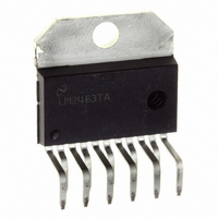
IC DRIVER MONOLITHIC TO-220-11
Manufacturer
National Semiconductor
Datasheet
1.LM2463TANOPB.pdf
(12 pages)
Specifications of LM2463TA/NOPB
Display Type
CRT
Current - Supply
50mA
Voltage - Supply
60 V ~ 85 V
Operating Temperature
-20°C ~ 100°C
Mounting Type
Through Hole
Package / Case
TO-220-11 (Bent and Staggered Leads)
Lead Free Status / RoHS Status
Lead free / RoHS Compliant
Interface
-
Configuration
-
Digits Or Characters
-
Other names
*LM2463TA
*LM2463TA/NOPB
LM2463TA
LM2463TANOPB
LM2463TANOPB
*LM2463TA/NOPB
LM2463TA
LM2463TANOPB
LM2463TANOPB


Theory of Operation
The LM2463 is a high voltage monolithic three channel CRT
driver suitable for high resolution display applications. The
LM2463 operates with 80V and 12V power supplies. The
part is housed in the industry standard 11-lead TO-220
molded plastic power package.
The circuit diagram of the LM2463 is shown in Figure 1 . The
PNP emitter follower, Q5, provides input buffering. Q1 and
Q2 form a fixed gain cascode amplifier with resistors R1 and
R2 setting the gain at −20. Emitter followers Q3 and Q4
isolate the high output impedance of the cascode stage from
the capacitance of the CRT cathode which decreases the
sensitivity of the device to load capacitance. Q6 provides
biasing to the output emitter follower stage to reduce cross-
over distortion at low signal levels.
Figure 2 shows a typical test circuit for evaluation of the
LM2463. This circuit is designed to allow testing of the
LM2463 in a 50
sive FET probe. In this test circuit, the two 2.49k
form a 200:1 wideband, low capacitance probe when con-
nected to a 50
50
is ac coupled to the base of Q5.
Application Hints
INTRODUCTION
National Semiconductor (NSC) is committed to provide ap-
plication information that assists our customers in obtaining
the best performance possible from our products. The fol-
lowing information is provided in order to support this com-
mitment. The reader should be aware that the optimization of
performance was done using a specific printed circuit board
designed at NSC. Variations in performance can be realized
due to physical changes in the printed circuit board and the
application. Therefore, the designer should know that com-
ponent value changes may be required in order to optimize
performance in a given application. The values shown in this
document can be used as a starting point for evaluation
purposes. When working with high bandwidth circuits, good
layout practices are also critical to achieving maximum per-
formance.
IMPORTANT INFORMATION
The LM2463 performance is targeted for the VGA (640 x
480) to UXGA (1600 x 1200, 70Hz) resolution market. The
application circuits shown in this document to optimize per-
formance and to protect against damage from CRT arcover
are designed specifically for the LM2463. If another member
of the LM246X family is used, please refer to its datasheet.
POWER SUPPLY BYPASS
Since the LM2463 is a wide bandwidth amplifier, proper
power supply bypassing is critical for optimum performance.
Improper power supply bypassing can result in large over-
shoot, ringing or oscillation. 0.1 µF capacitors should be
connected from the supply pins, V
close to the LM2463 as is practical. Additionally, a 47 µF or
larger electrolytic capacitor should be connected from both
supply pins to ground reasonably close to the LM2463.
ARC PROTECTION
During normal CRT operation, internal arcing may occasion-
ally occur. Spark gaps, in the range of 200V, connected from
the CRT cathodes to CRT ground will limit the maximum
oscilloscope input). The input signal from the generator
coaxial cable and a 50
environment without the use of an expen-
CC
and V
BB
load (such as a
, to ground, as
resistors
5
voltage, but to a value that is much higher than allowable on
the LM2463. This fast, high voltage, high energy pulse can
damage the LM2463 output stage. The application circuit
shown in Figure 9 is designed to help clamp the voltage at
the output of the LM2463 to a safe level. The clamp diodes,
D1 and D2, should have a fast transient response, high peak
current rating, low series impedance and low shunt capaci-
tance. FDH400 or equivalent diodes are recommended. Do
not use 1N4148 diodes for the clamp diodes. D1 and D2
should have short, low impedance connections to V
ground respectively. The cathode of D1 should be located
very close to a separately decoupled bypass capacitor (C3 in
Figure 9 ). The ground connection of D2 and the decoupling
capacitor should be very close to the LM2463 ground. This
will significantly reduce the high frequency voltage transients
that the LM2463 would be subjected to during an arcover
condition. Resistor R2 limits the arcover current that is seen
by the diodes while R1 limits the current into the LM2463 as
well as the voltage stress at the outputs of the device. R2
should be a
metal or carbon film type resistor. Having large value resis-
tors for R1 and R2 would be desirable, but this has the effect
of increasing rise and fall times. Inductor L1 is critical to
reduce the initial high frequency voltage levels that the
LM2463 would be subjected to. The inductor will not only
help protect the device but it will also help minimize rise and
fall times as well as minimize EMI. For proper arc protection,
it is important to not omit any of the arc protection compo-
nents shown in Figure 9 .
1
⁄
2
W solid carbon type resistor. R1 can be a
www.national.com
CC
1
and
⁄
4
W
Related parts for LM2463TA/NOPB
Image
Part Number
Description
Manufacturer
Datasheet
Request
R

Part Number:
Description:
Programmable Quad Bipolar Operational Amplifiers
Manufacturer:
ST Microelectronics, Inc.
Datasheet:

Part Number:
Description:
National Semiconductor [8-Bit D/A Converter]
Manufacturer:
National Semiconductor
Datasheet:
Part Number:
Description:
National Semiconductor [Media Coprocessor]
Manufacturer:
National Semiconductor
Datasheet:
Part Number:
Description:
Digitally Controlled Tone and Volume Circuit with Stereo Audio Power Amplifier, Microphone Preamp Stage and National 3D Sound
Manufacturer:
National Semiconductor
Datasheet:
Part Number:
Description:
Digitally Controlled Tone and Volume Circuit with Stereo Audio Power Amplifier, Microphone Preamp Stage and National 3D Sound
Manufacturer:
National Semiconductor
Datasheet:
Part Number:
Description:
AC97 Rev 2 Codec with Sample Rate Conversion and National 3D Sound
Manufacturer:
National Semiconductor
Part Number:
Description:
Manufacturer:
National Semiconductor
Datasheet:
Part Number:
Description:
Manufacturer:
National Semiconductor
Datasheet:
Part Number:
Description:
General Purpose, Low Voltage, Low Power, Rail-to-Rail Output Operational Amplifiers
Manufacturer:
National Semiconductor
Datasheet:
Part Number:
Description:
8-bit 20 MSPS flash A/D converter.
Manufacturer:
National Semiconductor
Datasheet:
Part Number:
Description:
Low Noise Quad Operational Amplifier
Manufacturer:
National Semiconductor
Datasheet:
Part Number:
Description:
Quad Differential Line Receivers
Manufacturer:
National Semiconductor
Datasheet:
Part Number:
Description:
Quad High Speed Trapezoidal? Bus Transceiver
Manufacturer:
National Semiconductor
Datasheet:
Part Number:
Description:
Dual Line Receiver
Manufacturer:
National Semiconductor
Datasheet: