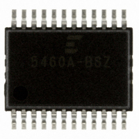
CS5460A-BSZ Cirrus Logic Inc, CS5460A-BSZ Datasheet - Page 42

CS5460A-BSZ
Manufacturer Part Number
CS5460A-BSZ
Description
IC ENERGY METERING 1PHASE 24SSOP
Manufacturer
Cirrus Logic Inc
Datasheet
1.CS5460A-BSZ.pdf
(54 pages)
Specifications of CS5460A-BSZ
Package / Case
24-SSOP
Input Impedance
30 KOhm
Measurement Error
0.1%
Voltage - I/o High
0.8V
Voltage - I/o Low
0.2V
Current - Supply
2.9mA
Voltage - Supply
4.75 V ~ 5.25 V
Operating Temperature
-40°C ~ 85°C
Mounting Type
Surface Mount
Meter Type
Single Phase
Output Voltage Range
2.4 V to 2.6 V
Output Current
1 uA
Input Voltage Range
2.4 V to 2.6 V
Input Current
25 nA
Power Dissipation
500 mW
Operating Temperature Range
- 40 C to + 85 C
Mounting Style
SMD/SMT
Ic Function
Single Phase Bi-directional Power / Energy IC
Brief Features
On-Chip Functions, AC Or DC System Calibration, Power Supply Monitor
Supply Voltage Range
3.3V To 5V
Rohs Compliant
Yes
Lead Free Status / RoHS Status
Lead free / RoHS Compliant
For Use With
CDB5460AU - EVALUATION BOARD FOR CS5460A
Lead Free Status / Rohs Status
Lead free / RoHS Compliant
Other names
598-1094-5
Available stocks
Company
Part Number
Manufacturer
Quantity
Price
Company:
Part Number:
CS5460A-BSZ
Manufacturer:
CIRRUS
Quantity:
2
Company:
Part Number:
CS5460A-BSZR
Manufacturer:
CIRRUS
Quantity:
8 000
Part Number:
CS5460A-BSZR
Manufacturer:
CIRRUS
Quantity:
20 000
4.2 Serial Port Interface
The CS5460A’s slave-mode serial interface con-
sists of two control lines and two data lines, which
have the following pin-names: CS, SCLK, SDI,
SDO. Each control line is now described.
CS Chip Select (input pin), is the control line which
enables access to the serial port. When CS is set
to logic 1, the SDI, SDO, and SCLK pins will be
held at high impedance. When the CS pin is set to
logic 0, the SDI, SDO, and SCLK pins have the fol-
lowing functionality:
SDI Serial Data In (input pin), is the user-generat-
ed signal used to transfer (send) data/com-
mand/address/etc. bits into the device.
SDO Serial Data Out (output pin), is the data sig-
nal used to read output data bits from the device’s
registers.
SCLK
bit-clock which controls the transfer rate of data
to/from the ADC’s serial port. To accommodate op-
to-isolators, SCLK is designed with a Schmitt-trig-
ger input to allow an opto-isolator with slower rise
and fall times to directly drive the pin. Additionally,
SDO is capable of sinking or sourcing up to 5 mA
to directly drive an opto-isolator LED. SDO will
have less than a 400 mV loss in the drive voltage
when sinking or sourcing 5 mA.
4.3 Serial Read and Write
The state machine decodes the command word as
it is received. Data is written to and read from the
CS5460A by using the Register Read/Write com-
mand. Figure 1 illustrates the serial sequence nec-
essary to write to or read from the serial port
buffers. As shown in Figure 1, a transfer of data is
always initiated by sending the appropriate 8-bit
command (MSB first) to the serial port (SDI pin). It
is important to note that some commands use in-
formation from the Cycle-Count Register and Con-
figuration Register to perform the function. For
those commands, it is important that the correct in-
formation is written to those registers first.
4.3.1 Register Write
When a command involves a write operation, the
serial port will continue to clock in the data bits
(MSB first) on the SDI pin for the next 24 SCLK cy-
cles. Command words instructing a register write
42
Serial Clock (input pin), is the serial
must be followed by 24 bits of data. For instance,
to write the Configuration Register, the command
(0x40) is transmitted to initiate a write to the Con-
figuration Register. The CS5460A will acquire the
serial data input from the SDI pin after 24 pulses
on the SCLK pin. Once the data is received, the
state machine writes the data to the Configuration
Register and then waits to receive another valid
command.
4.3.2 Register Read
When a read command is initiated, the serial port
will start transferring register content bits (MSB
first) on the SDO pin for the next 8, 16, or 24 SCLK
cycles. Command words instructing a register read
may be terminated at 8-bit boundaries (e.g., read
transfers may be 8, 16, or 24 bits in length). Also,
data register reads allow “command chaining”, in
which the micro-controller is allowed to send a new
command while reading register data. The new
command will be acted upon immediately and
could possibly terminate the first register read. For
example, if a command word is sent to the state
machine to read one of the output registers, then
after pulsing SCLK for 16-bits of data, a second
write command word (e.g., to clear the Status Reg-
ister) may be pulsed on to the SDI line at the same
time the last 8-bits of data (from the first read com-
mand) are pulsed from the SDO line.
During the read cycle, the SYNC0 command
(NOP) should be strobed on the SDI port while
clocking the data from the SDO port.
4.4 System Initialization
A software or hardware reset can be initiated at
any time. The software reset is initiated by writing
a logic 1 to the RS (Reset System) bit in the Con-
figuration Register, which automatically returns to
logic 0 after reset. At the end of the 32
(i.e., 8 bit command word and 24 bit data word) in-
ternal synchronization delays the loading of the
Configuration Register by 3 or 4 DCLK cycles.
Then the reset circuit initiates the reset routine on
the 1
A hardware reset is initiated when the RESET pin
is forced low for at least 50 ns. The RESET signal
is asynchronous, requiring no MCLKs for the part
to detect and store a reset event. The RESET pin
is a Schmitt Trigger input, which allows it to accept
st
falling edge of MCLK.
CS5460A
nd
DS487F4
SCLK


