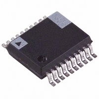
ADE7759ARSRL Analog Devices Inc, ADE7759ARSRL Datasheet - Page 31

ADE7759ARSRL
Manufacturer Part Number
ADE7759ARSRL
Description
IC ENERGY METERING 1PHASE 20SSOP
Manufacturer
Analog Devices Inc
Datasheet
1.ADE7759ARSZ.pdf
(36 pages)
Specifications of ADE7759ARSRL
Rohs Status
RoHS non-compliant
Input Impedance
390 KOhm
Measurement Error
0.1%
Voltage - I/o High
2.4V
Voltage - I/o Low
0.8V
Current - Supply
3mA
Voltage - Supply
4.75 V ~ 5.25 V
Operating Temperature
-40°C ~ 85°C
Mounting Type
Surface Mount
Package / Case
20-SSOP (0.200", 5.30mm Width)
Meter Type
Single Phase
For Use With
EVAL-ADE7759EBZ - BOARD EVALUATION FOR ADE7759
REV. A
Mode Register (06H)
The ADE7759 functionality is configured by writing to the mode register—see Figure 45. Table VI summarizes the functionality of
each bit in the mode register.
Bit
Location
0
1
2
3
4
5
6
7
8
9
10
12, 11
14, 13
15
Bit
Mnemonic
DISHPF
DISLPF2
DISCF
DISSAG
ASUSPEND
TEMPSEL
SWRST
CYCMODE
DISCH1
DISCH2
SWAP
DTRT1, 0
WAVSEL1, 0
TEST1
The HFP (high-pass filter) in Channel 1 is disabled when this bit is set.
The LPF (low-pass filter) after the multiplier (LPF2) is disabled when this bit is set.
The frequency output CF is disabled when this bit is set.
The line voltage sag detection is disabled when this bit is set.
By setting this bit to Logic 1, both ADE7759s’ A/D converters can be turned off. In normal
The temperature conversion starts when this bit is set to 1. This bit is automatically reset to
Software Chip Reset. A data transfer should not take place to the ADE7759 for at least 18 µs after
Setting this bit to Logic 1 places the chip in line cycle energy accumulation mode.
ADC 1 (Channel 1) inputs are internally shorted together.
ADC 2 (Channel 2) inputs are internally shorted together.
By setting this bit to Logic 1 the analog inputs V2P and V2N are connected to ADC 1 and the
These bits are used to select the waveform register update rate.
These bits are used to select the source of the sampled data for the waveform register.
Writing a Logic 1 to this bit position places the ADE7759 in test mode. This is intended for fac-
Description
operation, this bit should be left at Logic 0. All digital functionality can be stopped by suspending
the clock signal at CLKIN pin.
0 when the temperature conversion is finished.
a software reset.
analog inputs V1P and V1N are connected to ADC 2.
DTRT1
0
0
1
1
WAVSEL1, 0
0
0
1
1
tory testing only and should be left at 0.
0
1
0
1
DTRT0
0
1
0
1
Length
24 bits
40 bits
24 bits
24 bits
Table VI. Mode Register
Update Rate
27.9 kSPS (CLKIN/128)
14 kSPS (CLKIN/256)
7 kSPS (CLKIN/512)
3.5 kSPS (CLKIN/1024)
–31–
Source
Active Power Signal (output of LPF2)
Channel 1 and Channel 2
Channel 1
Channel 2
ADE7759


