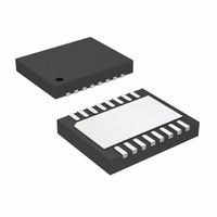
LTC4223CDHD-2#PBF Linear Technology, LTC4223CDHD-2#PBF Datasheet - Page 4

LTC4223CDHD-2#PBF
Manufacturer Part Number
LTC4223CDHD-2#PBF
Description
IC CNTRLR HOT SWAP DUAL 16-DFN
Manufacturer
Linear Technology
Type
Hot-Swap Controllerr
Datasheet
1.LTC4223CDHD-2PBF.pdf
(24 pages)
Specifications of LTC4223CDHD-2#PBF
Applications
ATCA, MicroTCA™
Internal Switch(s)
No
Voltage - Supply
2.7 V ~ 6 V
Operating Temperature
0°C ~ 70°C
Mounting Type
Surface Mount
Package / Case
16-WFDFN Exposed Pad
Lead Free Status / RoHS Status
Lead free / RoHS Compliant
Available stocks
Company
Part Number
Manufacturer
Quantity
Price
LTC4223-1/LTC4223-2
ELECTRICAL CHARACTERISTICS
temperature range, otherwise specifi cations are T
SYMBOL
I
I
Open Drain Outputs
V
V
I
Logic Inputs
V
I
R
Other Pin Functions
I
I
R
Propagation Delays
t
t
t
t
t
t
t
t
t
t
Note 1: Stresses beyond those listed under Absolute Maximum Ratings
may cause permanent damage to the device. Exposure to any Absolute
Maximum Rating condition for extended periods may affect device
reliability and lifetime.
Note 2: All currents into device pins are positive; all currents out of
the device pins are negative. All voltages are referenced to GND unless
otherwise specifi ed.
4
TMR(UP)
TMR(DN)
PU
IN(LEAK)
12VSENSE
12VOUT
CB
PHL(SENSE)
PHH(AUXON)
PHH(12ON)
RST(ON)
RST(VCC)
PLL(UVLO)
PHL(GATE)
PLH(PG)
P(12IMON)
OL
OH
IN(TH)
PU
OUT(DIS)
PARAMETER
TIMER Pull-Up Current
TIMER Pull-Down Current
Output Low Voltage ( ⎯ F ⎯ A ⎯ U ⎯ L ⎯ T , ⎯ 1 ⎯ 2 ⎯ P ⎯ G ⎯ O ⎯ O ⎯ D ,
⎯ A ⎯ U ⎯ X ⎯ P ⎯ G ⎯ O ⎯ O ⎯ D )
Output High Voltage ( ⎯ F ⎯ A ⎯ U ⎯ L ⎯ T , ⎯ 1 ⎯ 2 ⎯ P ⎯ G ⎯ O ⎯ O ⎯ D ,
⎯ A ⎯ U ⎯ X ⎯ P ⎯ G ⎯ O ⎯ O ⎯ D )
Output Pin Pull-Up Current ( ⎯ F ⎯ A ⎯ U ⎯ L ⎯ T ,
⎯ 1 ⎯ 2 ⎯ P ⎯ G ⎯ O ⎯ O ⎯ D , ⎯ A ⎯ U ⎯ X ⎯ P ⎯ G ⎯ O ⎯ O ⎯ D )
Logic Input Threshold (12ON, AUXON, ⎯ E ⎯ N )
Input Leakage Current (12ON, AUXON)
⎯ E ⎯ N Pin Pull-Up Resistance
12V
12V
OUT Pin Discharge Resistance
12V
AUXOUT
AUX Circuit Breaker Trip Delay
Sense Voltage, (12V
High to 12V
AUXON High to AUXOUT High
12ON High to 12V
Input Low (12ON, AUXON) to ⎯ F ⎯ A ⎯ U ⎯ L ⎯ T High
V
12V
AUXIN Low to ⎯ A ⎯ U ⎯ X ⎯ P ⎯ G ⎯ O ⎯ O ⎯ D High
⎯ E ⎯ N High to 12V
12V
AUXOUT Low to ⎯ A ⎯ U ⎯ X ⎯ P ⎯ G ⎯ O ⎯ O ⎯ D High
Input Sense Voltage Step to 12IMON
Propagation Delay
CC
SENSE
OUT
OUT
IN
OUT
Low to ⎯ F ⎯ A ⎯ U ⎯ L ⎯ T High
Low to 12V
Pin Input Current
Low to ⎯ 1 ⎯ 2 ⎯ P ⎯ G ⎯ O ⎯ O ⎯ D High
Pin Input Current
GATE
GATE
Low
GATE
GATE
IN
Low
– 12V
Low
High
SENSE
)
A
= 25°C, V
CONDITIONS
V
V
V
V
V
I
(Note 5)
V
V
V
Gate Drive On, V
Gate Drive Off
V
V
After Power Up
ΔV
ΔV
ΔV
OL
TIMER
TIMER
TIMER
TIMER
TIMER
PU
IN
12VSENSE
12VOUT
AUXVOUT
SENSE
SENSE
SENSE
The
= 3mA
= V
= 1.5V
CC
CC
= 1V, Initial Timing Cycle
= 0V, In AUX Fault Mode
= 0V, In 12V Fault Mode
= 2V, No Faults
= 2V, In Reset Mode
= 3.3V, V
●
= 6V
= 300mV, C
= 100mV, C
= 100mV
= 2V
= 12V
denotes the specifi cations which apply over the full operating
Note 3: An internal clamp limits the 12V
above 12V
the device.
Note 4: For the DFN package, the AUX switch on resistance, R
is guaranteed by correlation to wafer test measurements.
Note 5: The output pins ⎯ F ⎯ A ⎯ U ⎯ L ⎯ T , ⎯ 1 ⎯ 2 ⎯ P ⎯ G ⎯ O ⎯ O ⎯ D and ⎯ A ⎯ U ⎯ X ⎯ P ⎯ G ⎯ O ⎯ O ⎯ D have an internal
pull-up to V
when faster rise time is required or for V
12VOUT
AUXIN
12VGATE
12VGATE
= 12V
= 3.3V, V
OUT
CC
= 10nF
= 10nF
. Driving this pin to voltages beyond the clamp may damage
of 10μA. However, an external pull-up resistor may be used
12VIN
=12V, unless otherwise specifi ed. (Note 2)
●
●
●
●
●
●
●
●
●
●
●
●
●
●
●
●
●
●
●
●
●
●
●
●
●
●
●
●
V
–140
CC
MIN
400
375
1.3
0.8
–7
–7
–6
60
10
20
12
2
6
6
– 1
GATE
OH
voltages greater than V
pin to a minimum of 4.5V
–200
0.15
TYP
–10
–10
–10
100
800
750
0.5
50
50
25
15
30
20
80
12
12
20
20
20
2
8
5
2
MAX
–260
1600
1500
–13
–13
–14
140
100
100
150
2.6
0.4
16
±1
50
12
30
60
40
18
18
40
40
40
2
1
6
DS(ON)
CC
.
UNITS
422312f
limit
mA
kΩ
μA
μA
μA
μA
μA
μA
μA
μA
μs
μs
μs
μs
μs
μs
μs
μs
μs
μs
μs
μs
μs
Ω
Ω
V
V
V


