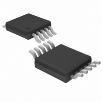
LTC4302CMS-1#PBF Linear Technology, LTC4302CMS-1#PBF Datasheet - Page 9

LTC4302CMS-1#PBF
Manufacturer Part Number
LTC4302CMS-1#PBF
Description
IC BUS BUFFER 2-WIRE 10-MSOP
Manufacturer
Linear Technology
Type
Hot-Swap Switchr
Datasheet
1.LTC4302CMS-1PBF.pdf
(20 pages)
Specifications of LTC4302CMS-1#PBF
Applications
General Purpose, Buffer/Bus Extender
Internal Switch(s)
Yes
Voltage - Supply
2.7 V ~ 5.5 V
Operating Temperature
0°C ~ 70°C
Mounting Type
Surface Mount
Package / Case
10-TFSOP, 10-MSOP (0.118", 3.00mm Width)
Lead Free Status / RoHS Status
Lead free / RoHS Compliant
Available stocks
Company
Part Number
Manufacturer
Quantity
Price
OPERATIO
broken up into 9-bit segments, one byte followed by one
bit for acknowledging. For example, sending out an ad-
dress consists of 7-bits of device address, 1-bit that
signals whether a read or write operation will be per-
formed and then 1 more bit to allow the slave to acknowl-
edge. There is no theoretical limit to how many total bytes
can be exchanged in a given transmission.
I
having been derived from I
targeted to low power devices (particularly battery pow-
ered ones) and emphasizes low power consumption while
I
consumption of the bus is not as critical. I
different specifications for three different maximum speeds,
these being standard mode (100kHz max), fast mode
(400kHz max), and Hs mode (3.4MHz max). Standard and
fast mode are not radically different, but Hs mode is very
different from a hardware and software perspective and
requires an initiating command at standard or fast speed
before data can start transferring at Hs speed. SMBus
simply specifies a 100kHz maximum speed.
The START and STOP Conditions
When the bus is not in use, both SCL and SDA must be
high. A bus master signals the beginning of a transmission
with a START condition by transitioning SDA from high to
low while SCL is high. When the master has finished
communicating with the slave, it issues a STOP condition
by transitioning SDA from low to high while SCL is high.
The bus is then free for another transmission.
Acknowledge
The acknowledge signal is used for handshaking between
the master and the slave. An acknowledge (LOW active)
generated by the slave lets the master know that the latest
2
2
C and SMBus are very similar specifications, SMBus
C is targeted to higher speed systems where the power
U
2
C. In general, SMBus is
R1
R2
V
CC
ADDRESS
4
Figure 1. Address Compare Circuitry
2
C has three
byte of information was received. The acknowledge re-
lated clock pulse is generated by the master. The transmit-
ter master releases the SDA line (HIGH) during the ac-
knowledge clock pulse. The slave-receiver must pull down
the SDA line during the acknowledge clock pulse so that it
remains stable LOW during the HIGH period of this clock
pulse.
When a slave-receiver doesn’t acknowledge the slave
address (for example, it’s unable to receive because it’s
performing a real-time function), the data line must be left
HIGH by the slave. The master can then generate a STOP
condition to abort the transfer.
If a slave receiver does acknowledge the slave address but
some time later in the transfer cannot receive any more
data bytes, the master must again abort the transfer. This
is indicated by the slave not generating the acknowledge
on the first byte to follow. The slave leaves the data line
HIGH and the master generates the STOP condition. When
the master is reading data from the slave, the master
acknowledges each byte read except for the last byte read.
The master signals a not acknowledge when no other data
is to be read and carries out the STOP condition.
Address Byte and Setting the LTC4302’s Address
The LTC4302’s address is set by connecting ADDRESS to
a resistive divider between V
ADDRESS is converted into a 5-bit digital word by an A/D
converter, as shown in Figure 1. This 5-bit word sets the
5 LSB’s of the LTC4302’s address; its two MSB’s are
always “11”. Using 1% resistors, the voltage at ADDRESS
is set 0.5LSB away from each code transition. For ex-
ample, with V
code. To set an address of 00, set ADDRESS to 0V +
0.5LSB = 78.125mV.
5-BIT
A/D
LTC4302-1/LTC4302-2
4302 F01
CC
=5V, 1LSB=5V/32 codes = 156.25mV/
5 WIRE
CC
and ground. The voltage on
sn430212 430212fs
9


