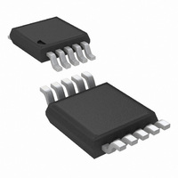
LM5067MM-1/NOPB National Semiconductor, LM5067MM-1/NOPB Datasheet - Page 21

LM5067MM-1/NOPB
Manufacturer Part Number
LM5067MM-1/NOPB
Description
IC CTLR NEG HOTSWAP LATCH 10MSOP
Manufacturer
National Semiconductor
Type
Hot-Swap Controllerr
Datasheet
1.LM5067MM-1NOPB.pdf
(24 pages)
Specifications of LM5067MM-1/NOPB
Applications
General Purpose
Internal Switch(s)
No
Voltage - Supply
-9 V ~ -80 V
Operating Temperature
-40°C ~ 125°C
Mounting Type
Surface Mount
Package / Case
10-TFSOP, 10-MSOP (0.118", 3.00mm Width)
For Use With
LM5067EVAL - NEGATIVE HOT SWAP / INRUSH CURRE
Lead Free Status / RoHS Status
Lead free / RoHS Compliant
Other names
LM5067MM-1TR
Available stocks
Company
Part Number
Manufacturer
Quantity
Price
Company:
Part Number:
LM5067MM-1/NOPB
Manufacturer:
NS
Quantity:
3 882
PC Board Guidelines
The following guidelines should be followed when designing
the PC board for the LM5067:
•
•
•
•
•
Place the LM5067 close to the board’s input connector to
minimize trace inductance from the connector to the FET.
Place R
transients below the Absolute Maximum rating of the
LM5067. Transients of several volts can easily occur when
the load current is shut off.
The sense resistor (R
and connected to it using the Kelvin techniques shown in
Figure 7.
The high current path from the board’s input to the load,
and the return path (via Q1), should be parallel and close
to each other wherever possible to minimize loop
inductance.
The VEE connection for the various components around
the LM5067 should be connected directly to each other,
and to the LM5067’s VEE pin, and then connected to the
IN
and C
IN
close to the VCC and VEE pins to keep
S
) should be close to the LM5067,
FIGURE 17. Suggested Board Connector Design
21
•
•
•
system VEE at one point. Do not connect the various
components to each other through the high current VEE
track.
Provide adequate heat sinking for the series pass device
(Q1) to help reduce thermal stresses during turn-on and
turn-off.
The board’s edge connector can be designed to shut off
the LM5067 as the board is removed, before the supply
voltage is disconnected from the LM5067. In Figure 17 the
voltage at the UVLO/EN pin goes to VEE before V
removed from the LM5067 due to the shorter edge
connector pin. When the board is inserted into the edge
connector, the system voltage is applied to the LM5067’s
VEE and VCC pins before voltage is applied to the UVLO/
EN pin.
If power dissipation within the LM5067 is high, an exposed
copper pad should be provided beneath the package, and
that pad should be connected to exposed copper on the
board’s other side with as many vias as possible. See the
Thermal Considerations section.
30030962
www.national.com
SYS
is


