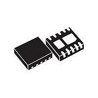
MAX5969BETB+T Maxim Integrated Products, MAX5969BETB+T Datasheet - Page 2

MAX5969BETB+T
Manufacturer Part Number
MAX5969BETB+T
Description
IC PWR OVER ETHERNET SW 10TDFN
Manufacturer
Maxim Integrated Products
Type
Power over Ethernet Switch (PoE)r
Datasheet
1.MAX5969BETBT.pdf
(14 pages)
Specifications of MAX5969BETB+T
Applications
Remote Peripherals (Industrial Controls, Cameras, Data Access)
Internal Switch(s)
Yes
Current Limit
Adjustable
Voltage - Supply
60V
Operating Temperature
-40°C ~ 85°C
Mounting Type
Surface Mount
Package / Case
10-WFDFN Exposed Pad
Lead Free Status / RoHS Status
Lead free / RoHS Compliant
Other names
MAX5969BETB+TTR
IEEE 802.3af/at-Compliant, Powered Device Interface
Controllers with
ABSOLUTE MAXIMUM RATINGS
V
DET, RTN, WAD, PG, 2EC to V
CLS to V
Maximum Current on CLS (100ms maximum) .................100mA
Continuous Power Dissipation (T
Note 1: Maximum power dissipation is obtained using JEDEC JESD51-5 and JESD51-7 specifications.
Note 2: Package thermal resistances were obtained using the method described in JEDEC specification JESD51-7, using a four-
Stresses beyond those listed under “Absolute Maximum Ratings” may cause permanent damage to the device. These are stress ratings only, and functional
operation of the device at these or any other conditions beyond those indicated in the operational sections of the specifications is not implied. Exposure to absolute
maximum rating conditions for extended periods may affect device reliability.
ELECTRICAL CHARACTERISTICS
(V
unless otherwise noted. T
2
DD
DETECTION MODE
Input Offset Current
Effective Differential Input
Resistance
CLASSIFICATION MODE
Classification Disable
Threshold
Classification Stability Time
Classification Current
TYPE 2 (802.3at) CLASSIFICATION MODE
Mark Event Threshold
Hysteresis on Mark Event
Threshold
Mark Event Current
Reset Event Threshold
POWER MODE
V
V
IN
10-Pin TDFN (derate 24.4mW/NC above +70NC)
Multilayer Board ........................................................1951mW
IN
IN
______________________________________________________________________________________
to V
= (V
Supply Voltage Range
Supply Current
SS
SS
layer board. For detailed information on package thermal considerations, refer to www.maxim-ic.com/thermal-tutorial.
DD
PARAMETER
..........................................................-0.3V to +100V
..............................................................-0.3V to +6V
- V
SS
) = 48V, R
A
DET
= T
SS
J
= 24.9kω, R
A
= -40
....................... -0.3V to +100V
= +70NC) (Note 1)
SYMBOL
V
I
I
OFFSET
I
TH,CLS
CLASS
V
V
MARK
N
dR
THM
THR
C to +85
I
Q
Integrated Power MOSFET
CLS
N
= 619ω. RTN, WAD, PG, and 2EC unconnected, all voltages are referenced to V
C, unless otherwise noted. Typical values are at T
V
V
V
V
V
20.5V, V
RTN = WAD =
PG = 2EC
V
V
P 10.1V
V
Measured at V
IN
IN
DD
IN
IN
IN
IN
IN
rising (Note 6)
= 1.4V to 10.1V (Note 4)
= 1.4V up to 10.1V with 1V step,
= 12.5V to
falling
falling to enter mark event, 5.2V P V
falling
= RTN = WAD = PG = 2EC (Note 5)
DD
=
CONDITIONS
DD
Package Thermal Resistance (Note 2)
Operating Temperature Range .......................... -40NC to +85NC
Maximum Junction Temperature .....................................+150NC
Storage Temperature Range ............................ -65NC to +150NC
Soldering Temperature (reflow) .................................... +260NC
Class 0, R
Class 1, R
Class 2, R
Class 3, R
Class 4, R
Class 5, R
B JA .................................................................................4NC/W
B JC ................................................................................9NC/W
CLS
CLS
CLS
CLS
CLS
CLS
= 619I
= 117I
= 66.5I
= 43.7I
= 30.9I
= 21.3I
IN
23.95
22.0
9.12
17.2
26.3
36.4
52.7
10.1
0.25
MIN
2.8
0
A
= +25
10.7
0.27
25.00
TYP
22.8
0.84
0.2
4
N
C.) (Note 3)
23.6
0.85
11.88
MAX
25.5
3.96
19.8
29.7
43.6
63.3
11.6
0.55
5.2
10
60
UNITS
mA
mA
mA
kI
ms
FA
V
V
V
V
V
SS,


