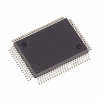
MAX5959AECS+ Maxim Integrated Products, MAX5959AECS+ Datasheet - Page 14

MAX5959AECS+
Manufacturer Part Number
MAX5959AECS+
Description
IC CTRLR HOT-PLUG QD 80-TQFP
Manufacturer
Maxim Integrated Products
Type
Hot-Swap Controllerr
Datasheet
1.MAX5959AECS.pdf
(25 pages)
Specifications of MAX5959AECS+
Applications
General Purpose, PCI Express
Internal Switch(s)
No
Voltage - Supply
3.3V, 12V
Operating Temperature
-40°C ~ 85°C
Mounting Type
Surface Mount
Package / Case
80-TQFP, 80-VQFP
Product
Controllers & Switches
Supply Voltage (max)
13 V
Supply Voltage (min)
3.3 V
Power Dissipation
1860 mW
Operating Temperature Range
- 40 C to + 85 C
Mounting Style
SMD/SMT
Supply Current
1 mA
Lead Free Status / RoHS Status
Lead free / RoHS Compliant
Quad PCI Express, Hot-Plug Controllers
The MAX5959/MAX5960 quad hot-plug controllers are
designed for PCIe applications. The devices provide
hot-plug control for 12V, 3.3V, and 3.3V auxiliary sup-
plies for three PCIe slots. The MAX5959/MAX5960s’
logic inputs/outputs allow interfacing directly with the
system hot-plug-management controller or through an
SMBus with an external I/O expander. An integrated
debounced attention switch and present-detect signals
are included to simplify system design (Figure 1).
14
67, 68
72, 73
PIN
63
64
65
74
75
76
77
78
79
______________________________________________________________________________________
3.3AUXOA
3.3AUXOB
PWRGDA
PWRGDB
FAULTA
FAULTB
3.3SB+
NAME
3.3SB-
3.3GA
3.3GB
12GB
Detailed Description
Slot A 3.3V Gate-Drive Output. Connect 3.3GA to the gate of slot A’s 3.3V MOSFET. At power-up,
V3.3GA is charged to 5.5V above the 3.3V supply by a constant current derived from V
rise time is determined by the external gate capacitance.
Open-Drain Fault Output Signal. FAULTA latches active low whenever slot A outputs are shut down due
to a fault. A fault is either of:
• An overcurrent condition lasting longer than the overcurrent timeout.
• A device over temperature condition.
If the fault is detected in the main outputs, FAULTA must be reset by toggling the ONA input. If the fault
is in the auxiliary output, FAULTA must be reset by toggling both ONA and AUXONA. For the autorestart
version, FAULTA is reset when the part initiates the next power-on cycle.
Open-Drain Power-Good Output. PWRGDA goes low 160ms after all outputs of slot A reach their final
value and the power MOSFETs are fully enhanced.
Slot A 3.3V Auxiliary Power-Supply Output
Slot B 3.3V Auxiliary Power-Supply Output
Open-Drain Power-Good Output. PWRGDB goes low 160ms after all outputs of slot B reach their final
value and the power MOSFETs are fully enhanced.
Open-Drain Fault Output Signal. FAULTB latches active-low whenever slot B outputs are shut down due
to a fault. A fault is either of:
• An overcurrent condition lasting longer than the overcurrent timeout.
• A device over temperature condition.
If the fault is detected in the main outputs, FAULTB must be reset by toggling the ONB input. If the fault
is in the auxiliary output, FAULTB must be reset by toggling both ONB and AUXONB. For the autorestart
version, FAULTB is reset when the part initiates the next power-on cycle.
Slot B 3.3V Gate-Drive Output. Connect 3.3GB to the gate of slot B’s 3.3V MOSFET. At power-up,
V
rise time is determined by the external gate capacitance.
Slot B 3.3V Negative Current-Sense Input. Connect to the negative side of the sense resistor using the
Kelvin-sensing technique to ensure accurate current sensing.
Slot B 3.3V Positive Current-Sense Input. Connect the positive side of the current-sense resistor to
3.3SB+ using the Kelvin-sensing technique to ensure accurate current sensing.
Slot B 12V Gate-Drive Output. Connect 12GB to the gate of slot B’s 12V MOSFET. At power-up, V
is raised to the internal charge-pump voltage level by a constant current.
3.3GB
is charged to 5.5V above the 3.3V supply by a constant current derived from V
The MAX5959/MAX5960 drive eight external n-chan-
nel MOSFETs to control the 12V and 3.3V main out-
puts. The 3.3V auxiliary outputs are controlled through
internal 0.2Ω n-channel MOSFETs. Internal charge
pumps provide a gate drive for the 12V outputs while
the gate drive of the 3.3V output is driven by the 12V
input supply. The 3.3V auxiliary outputs are complete-
ly independent from the main outputs with their own
charge pumps.
FUNCTION
Pin Description (continued)
12VIN
12VIN
. V
. V
3.3GB
3.3GA
12GB
‘s
‘s


