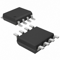
MAX5921FESA+ Maxim Integrated Products, MAX5921FESA+ Datasheet - Page 9

MAX5921FESA+
Manufacturer Part Number
MAX5921FESA+
Description
IC HOT-SWAP CTRLR -48V 8-SOIC
Manufacturer
Maxim Integrated Products
Type
Hot-Swap Controllerr
Datasheet
1.MAX5921FESA.pdf
(18 pages)
Specifications of MAX5921FESA+
Applications
General Purpose
Internal Switch(s)
No
Voltage - Supply
-20 V ~ -80 V
Operating Temperature
-40°C ~ 85°C
Mounting Type
Surface Mount
Package / Case
8-SOIC (0.154", 3.90mm Width)
Lead Free Status / RoHS Status
Lead free / RoHS Compliant
Figure 6a shows a typical hot-swap circuit for -48V sys-
tems. When the circuit board first makes contact with
the backplane, the DRAIN to GATE capacitance (C
of Q1 pulls up the GATE voltage to roughly IV
(C
internal dynamic clamp between GATE and V
keep the gate-to-source voltage of Q1 low during hot
insertion preventing Q1 from passing an uncontrolled
current to the load. For most applications, the internal
clamp between GATE and V
MAX5939 eliminates the need for an external gate-to-
source capacitor. The resistor R3 limits the current into
the clamp circuitry during card insertion.
The MAX5921/MAX5939 can reside either on the back-
plane or the removable circuit board (Figure 6a). Power
is delivered to the load by placing an external N-chan-
nel MOSFET pass transistor in the power-supply path.
After the circuit board is inserted into the backplane,
and the supply voltage at V
undervoltage and overvoltage tolerance, the
MAX5921/MAX5939 gradually turn on the external
MOSFET by charging the gate of Q1 with a 45µA cur-
rent source. Capacitor C2 provides a feedback signal
to accurately limit the inrush current.
Figure 6a. Inrush Control Circuitry/Typical Application Circuit
gd
/C
gd
SHORT PIN
-48V RTN
-48V RTN
+ C
-48V
gs
)I. The MAX5921/MAX5939 feature an
-48V Hot-Swap Controllers with External
_______________________________________________________________________________________
R
SENSE
4.7nF
Power-Supply Ramping
6.49kΩ
549kΩ
10kΩ
EE
1%
1%
1%
R4
R5
R6
is stable and within the
EE
Board Insertion
of the MAX5921/
UV
OV
and High Gate Pulldown Current
V
EE
0.02Ω
5%
R1
SENSE
EE
EE
gd
to
MAX5921
MAX5939
x
10Ω
)
5%
R2
V
DD
IRF530
GATE
Q1
The inrush current can be calculated:
where C
I
Figure 6b shows the inrush current waveform. The cur-
rent through C2 controls the GATE voltage. At the end
of the DRAIN ramp, the GATE voltage is charged to its
final value. The GATE-to-SENSE clamp limits the maxi-
mum ∆V
If the circuit card is removed from the backplane, the volt-
age at the UV falls below the UVLO detect threshold, and
the MAX5921/MAX5939 turn off the external MOSFET.
The MAX5921/MAX5939 provide current-limiting and cir-
cuit-breaker features that protect against excessive load
current and short-circuit conditions. The load current is
monitored by sensing the voltage across an external
sense resistor connected between V
PU
1kΩ
5%
R3
is the gate pullup current.
GATE
L
100V
15nF
C2
Current Limit and Electronic Circuit
is the total load capacitance, C3 + C4, and
DRAIN
PWRGD
to 18V.
100µF
100V
I
INRUSH
C4
0.1µF
100V
= I
C3
PU
x C
L
V
V
/ C2
EE
Board Removal
IN
IN
+
-
VI-J3D-CY
and SENSE.
GATE IN
VICOR
Breaker
9


