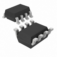
LTC4360CSC8-1#TRPBF Linear Technology, LTC4360CSC8-1#TRPBF Datasheet - Page 11

LTC4360CSC8-1#TRPBF
Manufacturer Part Number
LTC4360CSC8-1#TRPBF
Description
IC CTLR OVP 80V SHUTDOWN SC70-8
Manufacturer
Linear Technology
Type
Overvoltage Protection Controllerr
Datasheet
1.LTC4360CSC8-1TRMPBF.pdf
(14 pages)
Specifications of LTC4360CSC8-1#TRPBF
Applications
General Purpose
Internal Switch(s)
No
Voltage - Supply
2.5 V ~ 5.5 V
Operating Temperature
0°C ~ 70°C
Mounting Type
Surface Mount
Package / Case
8-VSSOP
Lead Free Status / RoHS Status
Lead free / RoHS Compliant
Available stocks
Company
Part Number
Manufacturer
Quantity
Price
APPLICATIONS INFORMATION
with the USB input already live. As shown in Figure 9, a
large current can build up in L
the N-channel MOSFET shuts off, the energy stored in L
is dumped into C
The LTC4360 limits this to a 1V rise in the output voltage.
If the voltage rise at V
energy in L
capability of the MOSFET is exceeded, an additional exter-
nal clamp such as the SMAJ24A can be placed between
IN and GND. C
protected circuits and its value will largely be determined
by their requirements. Using a larger C
L
IN
to slow down the dV/dt at OUT, allowing time for the
IN
into C
Figure 10. Recommended Layout for N-Channel MOSFET and P-/N-Channel MOSFET Configurations
OUT
OUT
OUT
, causing a large 40V input transient .
is the decoupling capacitor of the
is not acceptable or the avalanche
OUT
Figure 9. Overvoltage Protection Waveforms When 20V Plugged into 5V System
due to the discharge of the
IN
SUPPLY/IN
to charge up C
20V/DIV
10V/DIV
10A/DIV
OUT
1
2
3
4
5V/DIV
I
V
CABLE
LTC4360-1
Si1470DH
V
GATE
OUT
V
IN
will work with
FIGURE 8 CIRCUIT
R
LOAD = 10 , C
IN
OUT
8
7
6
5
= 150m , L
. When
OUT
GND
OUT
IN
IN
= 2µH
1µs/DIV
= 10µF (16V, SIZE 1210)
LTC4360 to shut off the MOSFET before V
to a dangerous voltage. A larger C
the ∆V
MOSFET BV
Layout Considerations
Figure 10 shows example PCB layouts for the single
N-channel MOSFET (SC70 package) configuration and the
P-channel MOSFET/N-channel MOSFET (Complementary
P , N MOSFET in TSOP-6 package) configuration. Keep the
traces to the MOSFETs wide and short. The PCB traces
associated with the power path through the MOSFETs
should have low resistance.
SUPPLY
IN
OUT
1
2
3
4
LTC4360-2
Si3590DV
436012 F08
due to the discharge of the energy in L
DSS
LTC4360-1/LTC4360-2
8
7
6
5
is used as an input clamp.
436012 F09
OUT
GND
OUT
also helps to lower
OUT
overshoots
11
IN
436012fa
if the


