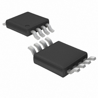
LTC4300-1CMS8 Linear Technology, LTC4300-1CMS8 Datasheet - Page 3

LTC4300-1CMS8
Manufacturer Part Number
LTC4300-1CMS8
Description
IC HOTSWAP 2WIRE BUS BUFFR 8MSOP
Manufacturer
Linear Technology
Type
Hot-Swap Switchr
Datasheet
1.LTC4300-1CMS8.pdf
(16 pages)
Specifications of LTC4300-1CMS8
Applications
General Purpose, Buffer/Bus Extender
Internal Switch(s)
Yes
Voltage - Supply
2.7 V ~ 5.5 V
Operating Temperature
0°C ~ 70°C
Mounting Type
Surface Mount
Package / Case
8-TSSOP, 8-MSOP (0.118", 3.00mm Width)
Lead Free Status / RoHS Status
Contains lead / RoHS non-compliant
Other names
Q1143786
Available stocks
Company
Part Number
Manufacturer
Quantity
Price
Company:
Part Number:
LTC4300-1CMS8
Manufacturer:
LT
Quantity:
5 321
Company:
Part Number:
LTC4300-1CMS8
Manufacturer:
LINEAR
Quantity:
16
Part Number:
LTC4300-1CMS8
Manufacturer:
LINEAR/凌特
Quantity:
20 000
Part Number:
LTC4300-1CMS8#PBF
Manufacturer:
LT/凌特
Quantity:
20 000
Part Number:
LTC4300-1CMS8#TRPBF
Manufacturer:
LT/凌特
Quantity:
20 000
ELECTRICAL CHARACTERISTICS
temperature range, otherwise specfications are at T
SYMBOL PARAMETER
Rise-Time Accelerators
I
V
V
I
t
Input-Output Connection
V
f
C
V
I
Timing Characteristics
f
t
t
t
t
t
t
t
t
t
t
Note 1: Absolute Maximum Ratings are those values beyond which the life
of a device may be impaired
Note 2: I
the Typical Performance Characteristics section.
Note 3: The connection circuitry always regulates its output to a higher
voltage than its input. The magnitude of this offset voltage as a function of
the pullup resistor and V
Characteristics section.
PULLUPAC
VACC
PDOFF
SCL, SDA
LEAK
I2C
BUF
hD,STA
su,STA
su,STO
hD, DAT
su, DAT
LOW
HIGH
f
r
ACCDIS
ACCEN
OS
IN
OL
PULLUPAC
Transient Boosted Pull-Up Current
Accelerator Disable Threshold
Accelerator Enable Threshold
ACC Input Current
ACC Delay, On/Off
Input-Output Offset Voltage
Operating Frequency
Digital Input Capacitance
Output Low Voltage, Input = 0V
Input Leakage Current
I
Bus Free Time Between Stop
and Start Condition
Hold Time After (Repeated)
Start Condition
Repeated Start Condition Setup Time
Stop Condition Setup Time
Data Hold Time
Data Setup Time
Clock Low Period
Clock High Period
Clock, Data Fall Time
Clock, Data Rise Time
2
C Operating Frequency
varies with temperature and V
CC
voltage is shown in the Typical Performance
CC
voltage, as shown in
CONDITIONS
Positive Transition on SDA,SCL, V
Slew Rate = 1.25V/ s (Note 2),
LTC4300-2, ACC = 0.7 • V
LTC4300-2
LTC4300-2
LTC4300-2
LTC4300-2
10k to V
LTC4300-2, V
Guaranteed by Design, Not Subject to Test
Guaranteed by Design, Not Subject to Test
SDA, SCL Pins, I
V
SDA, SCL Pins = V
LTC4300-2, V
(Note 4)
(Note 4)
(Note 4)
(Note 4)
(Note 4)
(Note 4)
(Note 4)
(Note 4)
(Note 4)
(Notes 4, 5)
(Notes 4, 5)
CC2
= 2.7V, LTC4300-2
A
CC
= 25 C. V
on SDA, SCL, V
CC2
CC2
The
SINK
= 3.3V, V
= 5.5V
CC
CC
= 3mA, V
= 5.5V,
denotes the specifications which apply over the full operating
= 2.7V to 5.5V, unless otherwise noted.
CC2
CC
IN
Note 4: Guaranteed by design, not subject to test.
Note 5: C
, V
= 0.2V
= 3.3V (Note 3),
CC
CC2
= 2.7V,
CC
= 2.7V
= 2.7V,
B
= total capacitance of one bus line in pF.
LTC4300-1/LTC4300-2
20 + 0.1 • C
20 + 0.1 • C
0.3 • V
MIN
300
100
1.3
0.6
0.6
0.6
1.3
0.6
1
0
0
0
0
CC2
B
B
0.5 • V
0.5 • V
TYP
75
0.1
2
5
CC2
CC2
0.7 • V
MAX
150
400
400
300
300
0.4
sn430012 430012fs
10
1
5
CC2
UNITS
3
kHz
kHz
mA
mV
ns
pF
ns
ns
ns
ns
V
V
A
V
A
s
s
s
s
s
s


