LTC4251-1CS6#TR Linear Technology, LTC4251-1CS6#TR Datasheet - Page 9

LTC4251-1CS6#TR
Manufacturer Part Number
LTC4251-1CS6#TR
Description
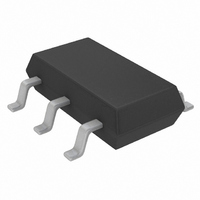
IC CTRLR HOTSWAP NEGVOLT SOT23-6
Manufacturer
Linear Technology
Type
Hot-Swap Controllerr
Datasheet
1.LTC4251CS6TRM.pdf
(24 pages)
Specifications of LTC4251-1CS6#TR
Applications
General Purpose
Internal Switch(s)
No
Voltage - Supply
-36 V ~ -72 V
Operating Temperature
0°C ~ 70°C
Mounting Type
Surface Mount
Package / Case
SOT-23-6 Thin, TSOT-23-6
Lead Free Status / RoHS Status
Contains lead / RoHS non-compliant
Other names
LTC4251-1CS6TR
LTC42511CS6TR
LTC42511CS6TR
Available stocks
Company
Part Number
Manufacturer
Quantity
Price
OPERATION
pin of the LTC4251-2. Secondly, all overvoltage conditions and references to OV, V
OV comparator in this part is disabled.
Hot Circuit Insertion
When circuit boards are inserted into a live backplane, the
supply bypass capacitors can draw huge transient currents
from the power bus as they charge. The flow of current
damages the connector pins and glitches the power bus,
causing other boards in the system to reset. The LTC4251/
LTC4251-1/LTC4251-2 are designed to turn on a circuit
board supply in a controlled manner, allowing insertion or
removal without glitches or connector damage.
Initial Start-Up
The LTC4251/LTC4251-1/LTC4251-2 reside on a removable
circuit board and control the path between the connector
and load or power conversion circuitry with an external
MOSFET switch (see Figure 1). Both inrush control and
short-circuit protection are provided by the MOSFET.
A detailed schematic is shown in Figure 2. –48V and
–48RTN receive power through the longest connector pins,
and are the first to connect when the board is inserted.
The GATE pin holds the MOSFET off during this time. UV/
OV determines whether or not the MOSFET should be
turned on based upon internal, high accuracy thresholds
and an external divider. UV/OV does double duty by also
monitoring whether or not the connector is seated. The top
of the divider detects –48RTN by way of a short connector
pin that is the last to mate during the insertion sequence.
BACKPLANE
–48RTN
–48V
Figure 1. Basic LTC4251 Hot Swap Topology
PLUG-IN BOARD
LTC4251
+
Note that for simplicity, the following assumptions are made in the text. Firstly, UV/OV also means the UV
C
LOAD
+
–
CONVERTER
ISOLATED
MODULE
DC/DC
+
–
LOW
VOLTAGE
CIRCUITRY
425112 F01
–48RTN
Interlock Conditions
A start-up sequence commences once five initial “interlock”
conditions are met:
1. The input voltage V
2. The voltage at UV/OV falls within the range of V
3. The (SENSE – V
4. The voltage on the timer capacitor (C
5. GATE is less than 0.5V (V
The first two conditions are continuously monitored and
the latter three are checked prior to initial timing or GATE
ramp-up. Upon exiting an OV condition, the TIMER pin
voltage requirement is inhibited. Details are described in
the Applications Information, Timing Waveforms section.
TIMER begins the start-up sequence by sourcing 5.8µA
into C
cycle stops and TIMER discharges C
then waits until the aforementioned conditions are once
again met. If C
low and GATE is released. GATE sources 58µA (I
charging the MOSFET gate and associated capacitance.
–48V
V
(V
SHORT
OVLO
LONG
LONG
TMRL
T
. If V
32.4k
402k
(UV > V
1%
1%
)
R1
R2
Figure 2. –48V, 2.5A Hot Swap Controller
OVHI
IN
LTC4251/LTC4251-1/
**DIODES, INC.
†RECOMMENDED FOR HARSH ENVIRONMENTS
and V
T
or UV/OV falls out of range, the start-up
successfully charges to 4V, TIMER pulls
C1
10nF
UVHI
EE
OVLO
) voltage is <50mV (V
, LTC4251-2)
D
DDZ13B**
IN
IN
†
do not apply to the LTC4251-2 as the
exceeds 9.2V (V
GATEL
C
1µF
IN
)
C
150nF
T
LTC4251-2
TIMER
UV/OV
V
EE
2
4
T
20m
18nF
C
T
R
C
to less than 1V,
S
) is less than 1V
LTC4251
LKO
SENSE
V
1
IN
CB
3
R
10k
500mW
)
10
IN
R
)
C
IRF530S
GATE
Q1
UVHI
+
GATE
415112fb
425112 F02
9
C
100µF
TYP
L
to
),


