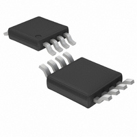
LTC4252-2CMS8#TR Linear Technology, LTC4252-2CMS8#TR Datasheet - Page 14

LTC4252-2CMS8#TR
Manufacturer Part Number
LTC4252-2CMS8#TR
Description
IC CNTRLR HOTSWAP NEGVOLT 8-MSOP
Manufacturer
Linear Technology
Type
Hot-Swap Controllerr
Specifications of LTC4252-2CMS8#TR
Applications
General Purpose
Internal Switch(s)
No
Operating Temperature
0°C ~ 70°C
Mounting Type
Surface Mount
Package / Case
8-TSSOP, 8-MSOP (0.118", 3.00mm Width)
Family Name
LTC4252-2
Package Type
MSOP
Operating Temperature (min)
0C
Operating Temperature (max)
70C
Operating Temperature Classification
Commercial
Product Depth (mm)
3mm
Product Height (mm)
0.86mm
Product Length (mm)
3mm
Mounting
Surface Mount
Pin Count
8
Lead Free Status / RoHS Status
Contains lead / RoHS non-compliant
Lead Free Status / RoHS Status
Contains lead / RoHS non-compliant
Other names
LTC4252-2CMS8TR
LTC42522CMS8TR
LTC42522CMS8TR
Available stocks
Company
Part Number
Manufacturer
Quantity
Price
APPLICATIO S I FOR ATIO
LTC4252-1/LTC4252-2
LTC4252A-1/LTC4252A-2
SHUNT REGULATOR
A fast responding regulator shunts the LTC4252 V
Power is derived from – 48RTN by an external current
limiting resistor. The shunt regulator clamps V
(V
transients and contributes a short delay at start-up. R
should be chosen to accommodate both V
rent and the drive required for an optocoupler if the
PWRGD function on the 10-pin MS package is used.
Higher current through R
for R
buffer driving the optocoupler as shown in Figure 3.
Multiple 1/4W resistors can replace a single higher power
R
INTERNAL UNDERVOLTAGE LOCKOUT (UVLO)
A hysteretic comparator, UVLO, monitors V
undervoltage. The thresholds are defined by V
hysteresis, V
enabled; below (V
pulled low. The UVLO function at V
confused with the UV/OV pin(s). These are completely
separate functions.
14
IN
Z
). A 1µF decoupling capacitor at V
resistor.
IN
and the LTC4252. An alternative is a separate NPN
LKH
. When V
LKO
U
(SHORT PIN)
– V
–48V
GND
GND
LKH
IN
IN
U
* M0C207
Q2: MMBT5551LT1
results in higher dissipation
rises above V
Figure 3. – 48V/2.5A Application with Different Input Operating Range
4.75k
38.3k
) it is disabled and GATE is
432k
1%
1%
1%
R1
R2
R3
W
C2
10nF
IN
IN
should not be
LKO
IN
filters supply
C
330nF
supply cur-
T
LKO
the chip is
U
IN
10
9
8
3
to 13V
and its
IN
IN
UV
OV
TIMER
SS
C
68nF
SS
pin.
for
IN
LTC4252-1
V
V
EE
IN
5
1
R
10k
1/2W
UV/OV COMPARATORS (LTC4252)
An UV hysteretic comparator detects undervoltage condi-
tions at the UV pin, with the following thresholds:
An OV hysteretic comparator detects overvoltage condi-
tions at the OV pin, with the following thresholds:
The UV and OV trip point ratio is designed to match the
standard telecom operating range of 43V to 82V when
connected together as in the typical application. A divider
(R1, R2) is used to scale the supply voltage. Using R1 =
402k and R2 = 32.4k gives a typical operating range of
43.2V to 82.5V. The undervoltage shutdown and overvolt-
age recovery thresholds are then 39.2V and 74.4V. 1%
divider resistors are recommended to preserve threshold
accuracy.
The R1-R2 divider values shown in the Typical Application
set a standing current of slightly more than 100µA and
define an impedance at UV/OV of 30kΩ. In most applica-
IN
PWRGD
SENSE
DRAIN
GATE
UV low-to-high (V
UV high-to-low (V
OV low-to-high (V
OV high-to-low (V
2
7
6
4
22k
C
1µF
R4
IN
R
D
1M
Q2
R5
2.2k
R
10Ω
C
100µF
C
18nF
UVHI
UVLO
OVHI
OVLO
C
*
C
L
+
) = 3.225V
) = 6.150V
) = 2.925V
) = 5.550V
Q1
IRF530S
4252-1/2 F03
R
0.02Ω
S
EN
LOAD
425212fb


