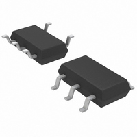
LTC4251-2IS6#TRMPBF Linear Technology, LTC4251-2IS6#TRMPBF Datasheet - Page 12

LTC4251-2IS6#TRMPBF
Manufacturer Part Number
LTC4251-2IS6#TRMPBF
Description
IC CTRLR HOTSWAP NEGVOLT SOT23-6
Manufacturer
Linear Technology
Type
Hot-Swap Controllerr
Datasheet
1.LTC4251CS6TRM.pdf
(24 pages)
Specifications of LTC4251-2IS6#TRMPBF
Applications
General Purpose
Internal Switch(s)
No
Voltage - Supply
-43V
Operating Temperature
-40°C ~ 85°C
Mounting Type
Surface Mount
Package / Case
SOT-23-6 Thin, TSOT-23-6
Lead Free Status / RoHS Status
Lead free / RoHS Compliant
Other names
LTC4251-2IS6#PBF
LTC4251-2IS6#PBF
LTC4251-2IS6#PBF
Available stocks
Company
Part Number
Manufacturer
Quantity
Price
APPLICATIONS INFORMATION
Overvoltage conditions detected by the OV comparator
will also pull GATE low, thereby shutting down the load,
but it will not reset the circuit breaker latch. Returning the
supply voltage to an acceptable range restarts the GATE
pin provided all interlock conditions except TIMER are met.
TIMER
The operation of the TIMER pin is somewhat complex as
it handles several key functions. A capacitor, C
at TIMER to provide timing for the LTC4251/LTC4251-1/
LTC4251-2. Four different charging and discharging modes
are available at TIMER:
1. 5.8µA slow charge; initial timing delay
2. 230µA fast charge; circuit breaker delay
3. 5.8µA slow discharge; circuit breaker “cool-off”
4. Low impedance switch; resets capacitor after initial
For initial startup, the 5.8µA pull-up is used. The low im-
pedance switch is turned off and the 5.8µA current source
is enabled when the four interlock conditions are met. C
charges to 4V in a time period given by:
When C
turns on and discharges C
and the load turns on.
CIRCUIT BREAKER TIMER OPERATION
If the SENSE pin detects more than 50mV across R
the TIMER pin charges C
4V, the GATE pin pulls low and the LTC4251/LTC4251-1/
LTC4251-2 latch off. The part remains latched off until
either the UV/OV pin is momentarily pulsed low, or V
dips into UVLO and is then restored. The circuit breaker
timeout period is given by
LTC4251/LTC4251-1/
LTC4251-2
12
timing delay, in undervoltage lockout, and in overvoltage
t =
t =
4V • C
4V • C
230µA
5.8µA
T
reaches 4V (V
T
T
TMRH
T
T
with 230µA. If C
. The GATE output is enabled
), the low impedance switch
T
charges to
T
, is used
(1)
(2)
IN
S
T
,
GATE
GATE is pulled low to V
conditions: in UVLO, during the initial timing cycle, in an
overvoltage condition, or when the LTC4251/LTC4251-1/
LTC4251-2 are latched off after a short-circuit. When GATE
turns on, a 58µA current source charges the MOSFET gate
and any associated external capacitance. V
drive to no more than 14.5V.
Gate-drain capacitance (C
abrupt application of power can cause a gate-source
voltage sufficient to turn on the MOSFET. A unique circuit
pulls GATE low with practically no usable voltage at V
and eliminates current spikes at insertion. A large external
gate-source capacitor is thus unnecessary for the purpose
of compensating C
capacitor C
for the analog current limit loop.
Intermittent overloads may exceed the 50mV threshold
at SENSE, but if their duration is sufficiently short TIMER
will not reach 4V and the LTC4251/LTC4251-1/LTC4251-2
will not latch off. To handle this situation, the TIMER
discharges C
the SENSE voltage is less than 50mV. Therefore any in-
termittent overload with an aggregate duty cycle of 2.5%
or more will eventually trip the circuit breaker and latch
off the LTC4251/LTC4251-1/LTC4251-2. Figure 3 shows
the circuit breaker response time in seconds normalized
to 1µF . The asymmetric charging and discharging of C
a fair gauge of MOSFET heating.
0.01
0.1
10
Figure 3. Circuit Breaker Response Time
1
C
0
is adequate. C
T
slowly with a 5.8µA pull-down whenever
20
FAULT DUTY CYCLE, D (%)
GD
C
T
(µF)
t
. Instead, a smaller value (≥10nF)
40
=
(235.8 • D) – 5.8
EE
GD
C
also provides compensation
under any of the following
) feed through at the first
60
4
80
425112 F03
100
IN
limits gate
425112fb
T
IN
is
,


