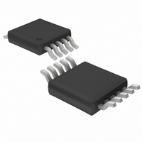
LTC4211CMS Linear Technology, LTC4211CMS Datasheet - Page 12

LTC4211CMS
Manufacturer Part Number
LTC4211CMS
Description
IC CONTROLLER HOT SWAP 10-MSOP
Manufacturer
Linear Technology
Type
Hot-Swap Controllerr
Datasheet
1.LTC4211IMS8PBF.pdf
(36 pages)
Specifications of LTC4211CMS
Applications
General Purpose
Internal Switch(s)
No
Voltage - Supply
2.5 V ~ 16.5 V
Operating Temperature
0°C ~ 70°C
Mounting Type
Surface Mount
Package / Case
10-TFSOP, 10-MSOP (0.118", 3.00mm Width)
Lead Free Status / RoHS Status
Contains lead / RoHS non-compliant
Available stocks
Company
Part Number
Manufacturer
Quantity
Price
Part Number:
LTC4211CMS
Manufacturer:
LT
Quantity:
20 000
Company:
Part Number:
LTC4211CMS#PBF
Manufacturer:
Linear Technology
Quantity:
1 971
Part Number:
LTC4211CMS#PBF
Manufacturer:
LT凌特厂
Quantity:
20 000
Company:
Part Number:
LTC4211CMS#TRPBF
Manufacturer:
TI
Quantity:
16 094
Part Number:
LTC4211CMS#TRPBF
Manufacturer:
MSOP-10
Quantity:
20 000
Company:
Part Number:
LTC4211CMS8
Manufacturer:
LT
Quantity:
10 000
Part Number:
LTC4211CMS8
Manufacturer:
LT/凌特
Quantity:
20 000
Part Number:
LTC4211CMS8#2KMPBF
Manufacturer:
LT/凌特
Quantity:
20 000
OPERATIO
LTC4211
HOT CIRCUIT INSERTION
When circuit boards are inserted into or removed from live
backplanes, the supply bypass capacitors can draw huge
transient currents from the backplane power bus as they
charge. The transient current can cause permanent dam-
age to the connector pins as well as cause glitches on the
system supply, causing other boards in the system to
reset.
The LTC4211 is designed to turn a printed circuit board’s
supply voltages ON and OFF in a controlled manner, allow-
ing the circuit board to be safely inserted or removed from
a live backplane. The device provides a system reset signal
to indicate when board supply voltage drops below a pre-
determined level, as well as a dual function fault monitor.
OUTPUT VOLTAGE MONITOR
The LTC4211 uses a 1.236V bandgap reference, precision
voltage comparator and an external resistor divider to
monitor the output supply voltage as shown in Figure 1.
The operation of the supply monitor in normal mode is il-
lustrated in Figure 2. When the supply voltage at the FB pin
drops below its reset threshold (1.236V), the comparator
12
ON/RESET
GND
V
U
CC
CONNECTOR
BACKPLANE
(FEMALE)
CONNECTOR
PCB EDGE
(MALE)
Figure 1. Supply Voltage Monitor Block Diagram
LONG
SHORT
LONG
2
ON
LTC4211
LOGIC
TIMER
TIMER
3
C
TIMER
V
CC
COMP2 output goes high. After passing through a glitch fil-
ter, RESET is pulled low (Time Point N2). When the voltage
at the FB pin rises above its reset threshold (1.239V),
COMP2’s output goes low and a timing cycle starts (Time
Point N4). After a complete timing cycle, RESET is pulled
high by the external pull-up resistor. If the FB pin rises above
the reset threshold for less than a timing cycle, the RESET
output remains low (Time Point N3).
As shown in Figure 5, the LTC4211’s RESET pin is logic
low during any undervoltage lockout condition and during
the initial insertion of a PC board. Under normal operation,
RESET goes to logic high at the end of the soft-start cycle
only after the FB pin voltage rises above its reset threshold
of 1.239V.
8
R
SENSE
REFERENCE
COMP2
SENSE
Figure 2. Supply Monitor Waveforms in Normal Mode
1.236V
7
TIMER
RESET
V
–
+
OUT
GATE
N1
Q1
6
N2
V1
4
Q2
GND
RESET
FB
V2
5
1
N3
R1
R2
V1
V2
R3
10k
4211 F01
RESET
N4
µP
POWER GOOD
+
DELAY
V
C
OUT
LOAD
1.236V
4211 F02
4211fa


