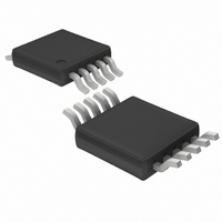
LTC4224IMS-2#TRPBF Linear Technology, LTC4224IMS-2#TRPBF Datasheet - Page 12

LTC4224IMS-2#TRPBF
Manufacturer Part Number
LTC4224IMS-2#TRPBF
Description
IC CNTRLR HOT SWAP DUAL 10-MSOP
Manufacturer
Linear Technology
Type
Hot-Swap Controllerr
Datasheet
1.LTC4224CDDB-2TRMPBF.pdf
(16 pages)
Specifications of LTC4224IMS-2#TRPBF
Applications
General Purpose
Internal Switch(s)
No
Voltage - Supply
1 V ~ 6 V
Operating Temperature
-40°C ~ 85°C
Mounting Type
Surface Mount
Package / Case
10-TFSOP, 10-MSOP (0.118", 3.00mm Width)
Lead Free Status / RoHS Status
Lead free / RoHS Compliant
Available stocks
Company
Part Number
Manufacturer
Quantity
Price
APPLICATIONS INFORMATION
LTC4224-1/LTC4224-2
Next, assume that there is no load current at start-up,
and calculate the inrush current required to charge the
load capacitor. As there is no gate capacitor, the supplies
start-up in current limit. Compute the time, t
to fully charge the load capacitor:
Table 3 lists the worst-case t
tolerance for load capacitances.
Table 3. Worst-Case t
The start-up ECB blanking delay is guaranteed to be at least
2.5ms, which is longer than the t
Hence, both supplies can start up successfully.
Next, verify that the thermal ratings of the selected external
MOSFETs are not exceeded during power-up or an output
short-circuit. Assuming the MOSFET dissipates power only
due to inrush current charging the load capacitor, the energy
dissipated in the MOSFET during power-up is the same
as that stored in the load capacitor after power-up. The
average power dissipated in the MOSFET is given by:
12
P
t
SU
AVG
VOLTAGE SUPPLY
=
=
V
3.3V
5V
CC
C
LOAD
I
TRIP
• C
2 • t
LOAD
• V
SU
SU
OUT
2
t
0.53ms
0.23ms
SU(MIN)
SU
SU
values assuming 30%
tabulated in Table 3.
t
0.65ms
0.29ms
SU(MAX)
SU
, it takes
The worst-case P
supply and the 3.3V supply. In this example, the FDS6911
MOSFET offers a good solution. Since this MOSFET is a dual
N-channel in a single SO8 package, it must be able to tolerate
the combined power dissipation of both supplies during
the t
temperature due to power dissipated in the MOSFET is
ΔT = P
Under this condition, the FDS6911 datasheet’s Transient
Thermal Impedance plot indicates that the junction tem-
perature will increase by 6.4°C using Z
(single pulse). The FDS6911’s on-resistance is 17mΩ at
V
The magnitude of the power pulse that results during a
severe overload is calculated to be 9.25W for the 5V sup-
ply and 9.2W for the 3.3V supply under the worst case
conditions. Assuming a worst-case circuit breaker timeout
period of 7.5ms, the junction temperature will increase by
25°C, with one supply short-circuited. If both supplies are
short-circuited, the junction temperature will increase by
50°C in the worst-case. During auto-retry (LTC4224-2), in
the event of persistent faults at both supplies, the ample
four second cooling delay limits the increase in junction
temperature to 50°C. The SOA curves of the FDS6911
indicate that the above conditions are safe.
GS
SU
= 4.5V, 25°C.
AVG
start-up time. The increase in steady-state junction
•Z
TH
where Z
AVG
is calculated to be 4.6W for both the 5V
TH
is the thermal impedance.
THJC
= 0.7°C/W
422412fa


