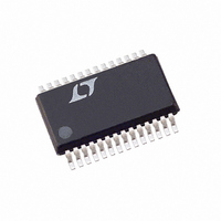
LTC4240CGN#PBF Linear Technology, LTC4240CGN#PBF Datasheet - Page 16

LTC4240CGN#PBF
Manufacturer Part Number
LTC4240CGN#PBF
Description
IC CTLR HOT SWAP CPCI I2C 28SSOP
Manufacturer
Linear Technology
Type
Hot-Swap Controllerr
Datasheet
1.LTC4240CGNPBF.pdf
(28 pages)
Specifications of LTC4240CGN#PBF
Applications
CompactPCI™
Internal Switch(s)
No
Voltage - Supply
3.3V, 5V, ±12V
Operating Temperature
0°C ~ 70°C
Mounting Type
Surface Mount
Package / Case
28-SSOP (0.150", 3.95mm Width)
Lead Free Status / RoHS Status
Lead free / RoHS Compliant
Available stocks
Company
Part Number
Manufacturer
Quantity
Price
LTC4240
APPLICATIO S I FOR ATIO
4. Short pins make contact. BD_SEL# signal connects to
Power-Up Sequence
Two external N-channel power MOSFETs isolate the 3.3V
and 5V power paths, while two internal MOS switches
isolate the 12V and –12V power paths. (See front page
Application Circuit). Sense resistors R1 and R2 provide
current limit and fault detection for the 3V
supplies, while R5 and C1 provide current control loop
compensation. Current fault detection for the 12V and
–12V supplies is done internally.
16
stage in the hot plug sequence, indicating that the
LTC4240 is in reset mode with all power switches off
(BD_SEL# is still pulled high to long 5V).
The 12V and –12V supplies make contact at this stage.
Zener clamps Z1 and Z2 plus shunt RC snubbers R13-
C4 and R14-C5 help protect the 12V
respectively, from large transient voltages during hot
insertion and short-circuit conditions.
The signal pins also connect at this point. This includes
the HEALTHY# signal connecting to the PWRGD pin
and the PCI_RST# signal connecting to the RESETIN
pin. The PWRGD and RESETIN signals are combined
internally with Bit 3 (C3) of the I
Send Byte protocol) to generate the LOCAL_PCI_RST#
signal, which is available at the RESETOUT pin.
the OFF/ON pin. This starts the electrical part of the
connection process. If the BD_SEL# signal is grounded
on the backplane, then the electrical connection pro-
cess starts immediately. Note that the electrical con-
nection process can be interrupted with the Send Byte
protocol of the I
System backplanes that do not ground the BD_SEL#
signal will instead have circuitry that detects when
BD_SEL# has made contact with the plug-in board. The
backplane logic can then control the power up process
by pulling BD_SEL# low. Figure 4 illustrates the power
up sequence. The mating of BD_SEL# is represented by
the high to low transition of the BD_SEL# signal.
2
U
C serial interface.
U
2
C command latch (see
W
IN
and V
IN
U
EEIN
and 5V
pins,
IN
A high to low transition on BD_SEL# causes the voltages
on the TIMER, GATE, 3V
pins to begin ramping (see Figure 4). The TIMER pin
capacitance is charged by an 11.5 A current source while
the GATE capacitance is charged by a 65 A current source.
Concurrently, an internal charge pump turns on the gates
of the internal power switches that isolate the 12V and
–12V supplies. All faults are ignored during the time that
the voltage at the TIMER pin remains below 5.5V. In order
to avoid faults due to the charging of the bulk output
capacitors, all output voltages must settle before the
TIMER pin reaches 5.5V. See TIMER section for more
details.
The 5V
ing to the slowest of the following slew rates:
LCL_PCI_RST#
dV
dt
HEALTHY#
BD_SEL#
10V/DIV
10V/DIV
10V/DIV
10V/DIV
10V/DIV
10V/DIV
OUT
12V
V
5V/DIV
5V/DIV
5V/DIV
TIMER
5V
3V
EEOUT
GATE
65
OUT
OUT
OUT
and 3V
C
Figure 4. Normal Power-Up Sequence
1
A
,
or
or
OUT
supply outputs will ramp up accord-
I
I
LIMIT V
LIMIT V
OUT
C
C
LOAD VOUT
LOAD VOUT
(
(
5
3
, 5V
10ms/DIV
)
)
–
–
(
(
OUT
5
3
I
I
LOAD V
LOAD V
, 12V
)
)
(
(
5
3
OUT
)
)
,
and V
4240 F04
EEOUT
( )
( )
1
1
a
b
4240f


