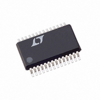
LTC4240IGN Linear Technology, LTC4240IGN Datasheet - Page 8

LTC4240IGN
Manufacturer Part Number
LTC4240IGN
Description
IC CTRLR HOT SWAP CPCI 28-SSOP
Manufacturer
Linear Technology
Type
Hot-Swap Controllerr
Datasheet
1.LTC4240CGNPBF.pdf
(28 pages)
Specifications of LTC4240IGN
Applications
CompactPCI™
Internal Switch(s)
No
Voltage - Supply
3.3V, 5V, ±12V
Operating Temperature
-40°C ~ 85°C
Mounting Type
Surface Mount
Package / Case
28-SSOP (0.150", 3.95mm Width)
Family Name
LTC4240
Package Type
SSOP N
Operating Supply Voltage (min)
2.55/4.45/10.8/-10.5V
Operating Supply Voltage (max)
5/12/14/-14V
Operating Temperature (min)
-40C
Operating Temperature (max)
85C
Operating Temperature Classification
Industrial
Product Depth (mm)
3.99mm
Product Height (mm)
1.5mm
Mounting
Surface Mount
Pin Count
28
Lead Free Status / RoHS Status
Contains lead / RoHS non-compliant
Lead Free Status / RoHS Status
Contains lead / RoHS non-compliant
Available stocks
Company
Part Number
Manufacturer
Quantity
Price
PI FU CTIO S
LTC4240
PRSNT1# (Pin 1): PCI Present Detect Input 1. PRSNT1#
and PRSNT2# are readable over the I
and PRSNT2# indicate the maximum power used by the
card. Do not float.
PRSNT2# (Pin 2): PCI Present Detect Input 2. Do not float.
12V
nally connected between 12V
current limit. An undervoltage lockout circuit prevents the
switches from turning on while the 12V
12V
circuitry. See Input Transient Protection section on how to
protect 12V
V
connected between V
rent limit. An undervoltage lockout circuit prevents the
switches from turning on while V
Connecting V
V
TIMER/AUX 12V
Input. Connect a capacitor from TIMER to GND. With the
LTC4240 turned off (OFF/ON = HIGH), the TIMER pin is
internally held at GND. When the device is turned on, an
11.5 A pull-up current source is connected to TIMER.
Current limit faults will be ignored until the voltage at the
TIMER pin rises above 5.5V. The Timer capacitor also
serves as an auxiliary charge reservoir for internal V
the event the 12V
UVL threshold voltage.
5V
pull low until the 5V
the power switches are turned off, a 50 resistor pulls
5V
FAULT (Pin 7): Open-Drain Fault Output . FAULT is pulled
low when a current limit fault is detected. Current limit
faults are ignored until the voltage at the TIMER pin is
above 5.5V. Once the TIMER cycle is complete, FAULT
pulls low and the LTC4240 turns off (in the event of an
overcurrent fault lasting longer than 35 s). The LTC4240
will remain in the off state until the OFF/ON pin is cycled
high then low or power is cycled. Note that the OFF/ON
cycling can also be performed using I
8
EEIN
EEOUT
OUT
OUT
U
IN
IN
(Pin 4): –12V Supply Input. A 1 internal switch is
(Pin 3): 12V Supply Input. A 0.5 switch is inter-
provides power to some of the LTC4240’s internal
(Pin 6): 5V Output Sense. The PWRGD pin will not
to ground.
. Also refer to Input Transient Protection section.
U
IN
EEIN
from large voltage transients.
IN
IN
section for more notes on V
pin voltage glitches below the LTC4240
OUT
(Pin 5): Current Fault Inhibit Timing
U
EEIN
pin voltage exceeds 4.65V. When
and V
IN
and 12V
EEOUT
EEIN
2
2
with foldback cur-
is above – 9V. See
IN
C bus.
C Bus. PRSNT1#
OUT
pin is below 8V.
with foldback
EEIN
CC
and
in
PWRGD (Pin 8): Open-Drain Power Good Output. Con-
nect the CPCI HEALTHY# signal to the PWRGD pin.
PWRGD remains low while V
2.9V, V
the supplies drops below its power good threshold volt-
age, PWRGD will go high after a 10 s deglitching time. The
switches will not be turned off when PWRGD goes high,
unless a fault has occurred. The CPCI specification calls
for a 0.01 F bypass capacitor on the backplane for
HEALTHY#.
BE (Pin 9): QuickSwitch Bus Enable Output. The BE output
remains high until power is good on all supplies. This
serves to isolate the I/O data lines during live
insertion. This is a CMOS output powered by 5V
GND (Pin 10): Analog Ground. Connect to analog ground
plane.
ADDRIN (Pin 11): I
I
pin to a resistor divider between the 5V
Table 1 for 1% resistor values and corresponding ad-
dresses. Resistors must be placed close to the ADDRIN
pin to minimize errors due to stray capacitance and
resistance on the board trace. Connect this pin to ground
if I
SDA (Pin 12): I
levels are used. Connect this pin to ground if I
used.
SCL (Pin 13): I
that TTL levels are used. Do not float. Connect this pin to
ground if I
RESETOUT (Pin 14): Open-Drain Reset Output. Connect
the CPCI LOCAL_PCI_RST# signal to the RESETOUT pin.
RESETOUT is the logical combination of RESETIN, PWRGD,
and I
LED (Pin 15): CPCI Status LED. Pulls low to light LED
when RESETOUT is low or when the I
DGND (Pin 16): Digital Ground. Connect to ground plane.
DRIVE (Pin 17): External transistor’s base drive output for
bus precharge. Connects to the base of an external NPN
emitter-follower which in turn biases the PRECHARGE
2
C address is programmed by connecting the ADDRIN
2
C is not used.
2
C RESETOUT latch output.
5VOUT
2
C is not used.
4.65V and V
2
2
C Data Input and Output. Note that TTL
C Clock Input, 100kHz Maximum. Note
2
C Address Programming Input. The
EEOUT
12VOUT
–10.5V. When any of
2
IN
C LED latch is set.
pin and GND. See
11.1V, V
2
IN
3VOUT
C is not
.
4240f


