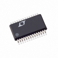
LTC4240IGN#TR Linear Technology, LTC4240IGN#TR Datasheet - Page 9

LTC4240IGN#TR
Manufacturer Part Number
LTC4240IGN#TR
Description
IC CTRLR HOT SWAP CPCI 28-SSOP
Manufacturer
Linear Technology
Type
Hot-Swap Controllerr
Datasheet
1.LTC4240CGNPBF.pdf
(28 pages)
Specifications of LTC4240IGN#TR
Applications
CompactPCI™
Internal Switch(s)
No
Voltage - Supply
3.3V, 5V, ±12V
Operating Temperature
-40°C ~ 85°C
Mounting Type
Surface Mount
Package / Case
28-SSOP (0.150", 3.95mm Width)
Lead Free Status / RoHS Status
Contains lead / RoHS non-compliant
Available stocks
Company
Part Number
Manufacturer
Quantity
Price
PI FU CTIO S
node. An external 1k resistor between the transistor’s base
and 3V
PRECHARGE (Pin 18): Precharge Monitor Input. An inter-
nal error amplifier servos the DRIVE pin voltage to keep the
precharge node at 1V. Becomes valid when long 5V and
3.3V power pins make contact .Tie pins 17 and 18 together
if precharge function is unused.
GATE (Pin 19): High Side Gate Drive for the External 3.3V
and 5V N-Channel Power Transistors. An external series
RC network is required for the current limit loop compen-
sation and to set the maximum ramp-up rate. During
power-up, the slope of the voltage rise at the GATE pin is
set by the 65 A current source charging the external GATE
capacitor or by the 3.3V or 5V current limit and the
associated output capacitor. During power-down, a 200 A
current source pulls the GATE pin to GND.
The voltage at the GATE pin will be modulated to maintain
a constant current when either the 3.3V or 5V supply goes
into current limit and the TIMER pin is less than 5.5V. Once
the TIMER pin is above 5.5V, and in the event of a current
fault condition lasting for longer than 35 s, the GATE pin
is immediately pulled to GND.
5V
placed between 5V
limit for this supply. A foldback current feature makes the
current limit decrease as the voltage at the 5V
approaches 0V. To disable the current limit, 5V
5V
5V
lockout circuit prevents the switches from turning on
when the voltage at the 5V
one long pin must be connected to 5V
output. See Input Transient Protection section.
3V
lockout circuit prevents the switches from turning on
when the voltage at the 3V
3.3V input supply is available, connect two series diodes
between 5V
cathode of second diode to 3V
SENSE
IN
IN
IN
U
must be tied together.
(Pin 22): 3.3V Supply Sense Input. An undervoltage
(Pin 21): 5V Supply Sense Input. An undervoltage
IN
(Pin 20): 5V Current Limit Sense. A sense resistor
is needed.
U
IN
and 3V
IN
U
IN
and 5V
(tie anode of first diode to 5V
IN
IN
SENSE
pin is less than 4.3V. At least
pin is less than 2.45V. If no
IN
, Figure 15). At least one
determines the current
IN
to ensure precharge
SENSE
OUT
IN
and
and
pin
long pin must be connected to 3V
output. See Input Transient Protection section.
3V
resistor placed between 3V
current limit for this supply. A foldback feature makes the
current limit decrease as the voltage at the 3V
approaches 0V. To disable current limit, 3V
must be tied together.
3V
cannot pull low until the 3V
If no 3.3V input supply is available, tie the 3V
5V
150 resistor pulls 3V
V
switch is connected between V
must exceed –10.5V before the PWRGD pin pulls low.
When the power switches are turned off, a 650 resistor
pulls V
12V
connected between 12V
exceed 11.1V before the PWRGD pin can pull low. When
the power switches are turned off, a 430 resistor pulls
12V
RESETIN (Pin 27): PCI Reset Input. Connect the CPCI
PCI_RST# signal to the RESETIN pin. Pulling RESETIN low
will cause RESETOUT to pull low. Note that the I
RESETIN latch output can also set RESETOUT. Do not
float.
OFF/ON (Pin 28): OFF/ON Input. Connect the CPCI
BD_SEL# signal to the OFF/ON pin. When the OFF/ON pin
is pulled low, the GATE pin is pulled high by a 65 A current
source and the internal 12V and –12V switches are turned
on. When the OFF/ON pin is pulled high, the GATE pin will
be pulled to ground by a 200 A current source and the 12V
and –12V switches turn off.
Cycling the OFF/ON pin high and low will reset a tripped
circuit breaker and start a new power-up sequence. The
I
electronic circuit breaker. Do not float.
2
EEOUT
C OFF/ON latch output can also be used to reset the
SENSE
OUT
OUT
OUT
OUT
EEOUT
pin. When the power switches are turned off, a
(Pin 24): 3.3V Output Sense. The PWRGD pin
(Pin 25): –12V Supply Output. An internal 1
to ground.
(Pin 26): 12V Supply Output. A 0.5 switch is
(Pin 23): 3.3V Current Limit Sense. A sense
to ground.
OUT
IN
IN
OUT
to ground.
and 12V
and 3V
pin voltage exceeds 2.9V.
EEIN
IN
SENSE
to ensure precharge
and V
OUT
LTC4240
. 12V
determines the
SENSE
EEOUT
OUT
OUT
pin to the
and 3V
. V
OUT
EEOUT
must
9
4240f
pin
2
IN
C


