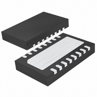
LTC4217CDHC#PBF Linear Technology, LTC4217CDHC#PBF Datasheet - Page 11

LTC4217CDHC#PBF
Manufacturer Part Number
LTC4217CDHC#PBF
Description
IC CTRLR HOT SWAP 2A 16-DFN
Manufacturer
Linear Technology
Type
Hot-Swap Switchr
Datasheet
1.LTC4217IFEPBF.pdf
(18 pages)
Specifications of LTC4217CDHC#PBF
Applications
General Purpose
Internal Switch(s)
Yes
Current Limit
2.0A
Voltage - Supply
2.9 V ~ 26.5 V
Operating Temperature
0°C ~ 70°C
Mounting Type
Surface Mount
Package / Case
16-WFDFN Exposed Pad
Linear Misc Type
Positive Low Voltage
Package Type
DFN EP
Operating Supply Voltage (min)
2.9V
Operating Temperature (min)
0C
Operating Temperature (max)
70C
Operating Temperature Classification
Commercial
Product Depth (mm)
3mm
Product Length (mm)
5mm
Mounting
Surface Mount
Pin Count
16
Lead Free Status / RoHS Status
Lead free / RoHS Compliant
Available stocks
Company
Part Number
Manufacturer
Quantity
Price
APPLICATIONS INFORMATION
over temperature. Normally the switch is turned off with
a 250µA current pulling down the GATE pin to ground.
With the switch turned off, the OUT voltage drops which
pulls the FB pin below its threshold. PG then pulls low to
indicate output power is no longer good.
If V
drops below 2.5V for greater than 1µs, a fast shutdown
of the switch is initiated. The GATE is pulled down with a
170mA current to the OUT pin.
Overcurrent Fault
The LTC4217 features an adjustable current limit with
foldback that protects against short-circuits or excessive
load current. To prevent excessive power dissipation in the
switch during active current limit, the available current is
reduced as a function of the output voltage sensed by the
FB pin. A graph in the Typical Performance Characteristics
curves shows the current limit versus FB voltage.
An overcurrent fault occurs when the current limit circuitry
has been engaged for longer than the timeout delay set
by the TIMER. Current limiting begins when the MOSFET
current reaches 0.5A to 2A (depending on the foldback).
The GATE pin is then brought down with a 140mA GATE-
to-OUT current. The voltage on the GATE is regulated in
order to limit the current to less than 2A. At this point, a
circuit breaker time delay starts by charging the external
timing capacitor from the TIMER pin with a 100µA pull-
up current. If the TIMER pin reaches its 1.2V threshold,
the internal switch turns off (with a 250µA current from
GATE to ground). Included in the Typical Performance
Characteristics curves is a graph of the Safe Operating
Area for the MOSFET. From this graph one can determine
the MOSFET’s maximum time in current limit for a given
output power.
DD
drops below 2.65V for greater than 5µs or INTV
Figure 3. Compensation for Small C
LTC4217
GATE
4217 F03
C
2.2nF
P
*OPTIONAL
RC TO LOWER
INRUSH CURRENT
LOAD
CC
Tying the TIMER pin to INTV
the internally generated (circuit breaker) delay of 2ms.
In either case the FLT pin is pulled low to indicate an
overcurrent fault has turned off the pass MOSFET. For a
given the circuit breaker time delay, the equation for set-
ting the timing capacitor’s value is as follows:
After the switch is turned off, the TIMER pin begins
discharging the timing capacitor with a 2µA pull-down
current. When the TIMER pin reaches its 0.2V threshold,
an internal 100ms timer is started. After the 100ms delay,
the switch is allowed to turn on again if the overcurrent
fault has been cleared. Bringing the UV pin below 0.6V
and then high will clear the fault. If the TIMER pin is tied
to INTV
an internal 100ms delay) if the overcurrent fault is cleared.
Tying the FLT pin to the UV pin allows the part to self-
clear the fault and turn the MOSFET on as soon as TIMER
pin has ramped below 0.2V. In this auto-retry mode the
LTC4217 repeatedly tries to turn on after an overcurrent
at a period determined by the capacitor on the TIMER pin.
The auto-retry mode also functions when the TIMER pin
is tied to INTV
The waveform in Figure 4 shows how the output latches
off following a short-circuit. The current in the MOSFET
is 0.5A as the timer ramps up.
Current Limit Adjustment
The default value of the active current limit is 2A. The
current limit threshold can be adjusted lower by placing
C
T
10V/DIV
10V/DIV
= t
∆V
1A/DIV
2V/DIV
TIMER
CC
V
GATE
I
OUT
OUT
CB
then the switch is allowed to turn on again (after
• 0.083(µF/ms)
Figure 4. Short-Circuit Waveform
CC
.
1ms/DIV
CC
will force the part to use
LTC4217
4217 F04
11
4217fd


