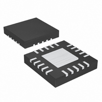
MAX3795ETG+ Maxim Integrated Products, MAX3795ETG+ Datasheet - Page 12

MAX3795ETG+
Manufacturer Part Number
MAX3795ETG+
Description
IC DRIVER VCSEL W/MON 24-TQFN
Manufacturer
Maxim Integrated Products
Type
Laser Diode Driverr
Datasheet
1.MAX3795ETG.pdf
(15 pages)
Specifications of MAX3795ETG+
Data Rate
4.25Gbps
Number Of Channels
1
Voltage - Supply
2.97 V ~ 3.63 V
Current - Supply
71mA
Current - Modulation
15mA
Current - Bias
15mA
Operating Temperature
-40°C ~ 85°C
Package / Case
24-TQFN Exposed Pad
Mounting Type
Surface Mount
Operating Supply Voltage
3.3 V
Minimum Operating Temperature
- 40 C
Mounting Style
SMD/SMT
Lead Free Status / RoHS Status
Lead free / RoHS Compliant
1Gbps to 4.25Gbps Multirate VCSEL Driver
with Diagnostic Monitors
current. For appropriate R
the Typical Operating Characteristics.
Select a communications-grade laser with a rise time of
90ps or better for 4.25Gbps applications. Use a high-
efficiency laser that requires low modulation current and
generates a low-voltage swing. Trim the leads to reduce
laser package inductance. The typical package leads
have inductance of 25nH per inch (1nH/mm). This
inductance causes a large voltage swing across the
laser. A compensation filter network can also be used to
reduce ringing, edge speed, and voltage swing.
A resistor (R
and ground controls the modulation current out of the
MAX3795 to the VCSEL. The modulation current is
given by the following:
It is important to note that the load impedance of the
VCSEL affects the modulation current being sourced by
the MAX3795. The Modulation Current vs. R
graph in the Typical Operating Characteristics shows the
current into a 50Ω load. Capacitance at the MODSET pin
should be ≤20pF.
The bias current output of the MAX3795 is controlled by
a resistor (R
and ground. In open-loop operation, BIASSET controls
the bias current level of the VCSEL. In closed-loop
operation (APC); the R
allowed bias current. The open-loop bias current is
given by the following:
The Bias Current vs. R
Operating Characteristics shows the current into a 50Ω
load. Capacitance at the BIASSET pin should be
≤20pF.
12
I
MOD
______________________________________________________________________________________
=
200
I
MODSET
BIASSET
BIAS
Programming Modulation Current
+
R
=
MODSET
1
) placed between the BIASSET pin
) placed between the MODSET pin
200
Programming Bias Current
BIASSET
+
BIASSET
R
TC
1 2
Design Procedure
×
BIASSET
.
and R
40
controls the maximum
graph in the Typical
×
MODSET
×
R
OUT
34
Select Laser
R
OUT
+
values, see
R
LOAD
MODSET
Compute the required modulation tempco from the
slope efficiency of the laser at T
higher temperature. Then select the value of R
the Typical Operating Characteristics. For example,
suppose a laser has a slope efficiency (SE) of
0.021mW/mA at +25°C, which reduces to 0.018mW/mA
at +85°C. The temperature coefficient is given by the
following:
From the Typical Operating Characteristics, the value
of R
modulation temperature compensation is not desired,
short TC1 and TC2.
Program the average optical power by adjusting
R
desired monitor current to be maintained over tempera-
ture and lifetime. See the Monitor Diode Current vs.
R
and select the value of R
required current.
Figure 4. Simplified Input Structure
Programming Modulation-Current Tempco
PWRSET
PWRSET
IN+
IN-
TC
PACKAGE
, which offsets the tempco of the laser, is 9kΩ. If
MAX3795
Laser tempco
1nH
1nH
graph in the Typical Operating Characteristics,
. To select the resistance, determine the
0.5pF
0.5pF
Programming the APC Loop
V
V
=
CC
CC
PWRSET
SE
=
(
SE
50Ω
50Ω
−
25
2380
85
×
1kΩ
−
(
ppm C
85 25
that corresponds to the
SE
A
−
25
V
= +25°C and at a
/
CC
°
)
)
×
15pF
10
6
TC
from


