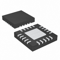
MAX3656ETG+T Maxim Integrated Products, MAX3656ETG+T Datasheet

MAX3656ETG+T
Specifications of MAX3656ETG+T
MAX3656ETG+TTR
Related parts for MAX3656ETG+T
MAX3656ETG+T Summary of contents
Page 1
... THIN QFN *EXPOSED PAD IS CONNECTED TO GND ________________________________________________________________ Maxim Integrated Products For pricing, delivery, and ordering information, please contact Maxim Direct at 1-888-629-4642, or visit Maxim’s website at www.maxim-ic.com. 155Mbps to 2.5Gbps Burst-Mode ♦ Multirate Operation from 155Mbps to 2.5Gbps ♦ Burst Enable/Disable Delay <2ns ♦ Burst On-Time of 576ns to Infinity ♦ ...
Page 2
Burst-Mode Laser Driver ABSOLUTE MAXIMUM RATINGS Supply Voltage, V ..............................................-0.5V to +6.0V CC Current into BIAS+, BIAS-, OUT+, OUT- ........-20mA to +150mA Current into MD.................................................... -5mA to +5mA Current into FAIL ...............................................-10mA to +10mA Voltage at IN+, ...
Page 3
ELECTRICAL CHARACTERISTICS (continued) (Typical values are +3.3V BIAS PARAMETER SYMBOL V BEN+ Single-Ended Input Voltage V BEN- Input High Voltage V IH Input Low Voltage V Output High Voltage V OH Output Low Voltage V ...
Page 4
Burst-Mode Laser Driver ELECTRICAL CHARACTERISTICS (continued) (Typical values are +3.3V BIAS PARAMETER SYMBOL BURST-MODE SPECIFICATIONS Burst Enable Delay Burst Disable Delay Burst On-Time (Note 13) t B-ON Burst Off-Time (Note 13) t ...
Page 5
BEN+ BEN- I BIAS + I MOD 10 ENABLE DELAY Figure 1. Enable and Disable Delay Times (T = +25°C, unless otherwise noted.) A OPTICAL EYE DIAGRAM (155.52Mbps, 117MHz FILTER, 23 PATTERN = PRBS) MAX3656 ...
Page 6
Burst-Mode Laser Driver (T = +25°C, unless otherwise noted.) A OPTICAL EYE DIAGRAM (2.48832Gbps, 2.3GHz FILTER, 23 PATTERN = PRBS) MAX3656 toc04 EXCELIGHT SLT2886-LR LASER AVERAGE OPTICAL POWER = -6dBm EXTINCTION RATIO = 10dB ...
Page 7
APCSET 10,000 1000 100 10 0 (kΩ) APCSET TIMING DIAGRAM, BURST ON V MOD+ V BIAS+ 500ps/div _______________________________________________________________________________________ 155Mbps to 2.5Gbps Burst-Mode Typical Operating Characteristics (continued) ...
Page 8
Burst-Mode Laser Driver PIN NAME Power-Supply Voltage CC 15, 18 IN+ Noninverting Data Input with On-Chip Biasing 3 IN- Inverting Data Input with On-Chip Biasing 5 BEN+ Noninverting Burst-Enable Input with ...
Page 9
Detailed Description The MAX3656 laser driver has three main parts: a high- speed modulator, a high-speed bias driver, and a laser- biasing block with automatic power control (see the Functional Diagram ). Both the bias and modulation output stages are ...
Page 10
Burst-Mode Laser Driver APC loop reset), and then it is driven low (chip- enabled). In this case, APC loop initialization begins when the voltage at EN drops below the specified EN input low voltage of 0.8V. After ...
Page 11
Programming the APC Loop When using the MAX3656’s APC feature, program the average optical power by adjusting the APCSET resis- tor. To select this resistor, determine the desired moni- tor current to be maintained over temperature and lifetime. See the ...
Page 12
Burst-Mode Laser Driver Design Example Select a communication-grade laser for the proper data rate. Assume the laser output average power is P 0dBm, the operating temperature is -40°C to +85°C and the laser diode has the following ...
Page 13
R = 5kΩ 3 LVTTL OR LVCMOS HIGH R = 3kΩ 4 LVTTL OR LVCMOS LOW R = 5kΩ 9kΩ 6 Figure 7. Single-Ended LVTTL or LVCMOS Biasing for Burst Enable Applications Information Running Burst Enable Single-Ended ...
Page 14
Burst-Mode Laser Driver MAX3656 IN+ IN- BEN+ BEN- R MODSET Chip Information TRANSISTOR COUNT: 8153 PROCESS: SiGe BIPOLAR 14 ______________________________________________________________________________________ I MOD I BIAS APC DAC DSP ASP R R LONGB BIASMAX EN FAIL APCSET Package Information ...
Page 15
... Maxim cannot assume responsibility for use of any circuitry other than circuitry entirely embodied in a Maxim product. No circuit patent licenses are implied. Maxim reserves the right to change the circuitry and specifications without notice at any time. Maxim Integrated Products, 120 San Gabriel Drive, Sunnyvale, CA 94086 408-737-7600 ____________________ 15 © 2010 Maxim Integrated Products 155Mbps to 2 ...


