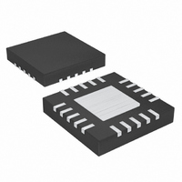
MAX3273ETG+T Maxim Integrated Products, MAX3273ETG+T Datasheet - Page 9

MAX3273ETG+T
Manufacturer Part Number
MAX3273ETG+T
Description
IC LASR DRVR 2.7GBPS 3.6V 24TQFN
Manufacturer
Maxim Integrated Products
Type
Laser Diode Driver (Fiber Optic)r
Datasheet
1.MAX3273ETG.pdf
(18 pages)
Specifications of MAX3273ETG+T
Data Rate
2.7Gbps
Number Of Channels
1
Voltage - Supply
3.14 V ~ 3.6 V
Current - Supply
30mA
Current - Modulation
60mA
Current - Bias
100mA
Operating Temperature
-40°C ~ 85°C
Package / Case
24-TQFN Exposed Pad
Mounting Type
Surface Mount
Lead Free Status / RoHS Status
Lead free / RoHS Compliant
optical output ringing and duty-cycle distortion. Refer to
Maxim application note HFAN 02.0, Interfacing Maxim
Laser Drivers with Laser Diodes, for more information.
At the data rate of 2.5Gbps, any capacitive load at the
cathode of a laser diode degrades the optical output
performance. Because the BIAS output is directly con-
nected to the laser cathode, the parasitic capacitance
associated with this pin is minimized by using an induc-
tor to isolate the BIAS pin from the laser cathode.
To maintain constant average optical power, the
MAX3273 incorporates an APC loop to compensate for
the changes in laser threshold current over temperature
and lifetime. A back-facet photodiode mounted in the
laser package is used to convert the optical power into
a photocurrent. The APC loop adjusts the laser bias
current so that the monitor current is matched to a ref-
erence current set by R
the APC loop is determined by an external capacitor
(C
associated with the APC loop-time constant, and to
guarantee loop stability, the recommended value for
C
When the APC loop is functioning, the maximum allow-
able bias current is set by an external resistor, R
An APC failure flag (FAIL) is asserted low when the bias
current can no longer be adjusted to achieve the desired
average optical power.
APC closed-loop operation requires the user to set three
currents with external resistors connected between
ground and BIASMAX, MODSET, and APCSET (see
Figure 3). Detailed guidelines for these resistor settings
are described in the Design Procedure section.
If necessary, the MAX3273 is fully operational without
APC. To disable the APC loop, ground the APCFILT1
pin. In this case, the laser current is directly set by two
external resistors connected from ground to BIASMAX
and MODSET. See the Design Procedure section for
more details on open-loop operation.
To minimize jitter in the input data, connect a synchro-
nous differential clock signal to the CLK+ and CLK-
inputs. When the LATCH control input is tied high, the
input data is retimed on the rising edge of CLK+. If
LATCH is tied low or left floating, the retiming function is
disabled and the input data is directly connected to the
output stage. When this latch function is not used, con-
nect CLK+ to V
APCFILT
APCFILT
is 0.01µF.
). To minimize the pattern-dependent jitter
Automatic Power Control (APC)
CC
and leave CLK- unconnected.
_______________________________________________________________________________________
+3.3V, 2.5Gbps Low-Power Laser Driver
Optional Data Input Latch
APCSET
Open-Loop Operation
. The time constant of
BIASMAX
.
The MAX3273 incorporates a TTL/CMOS input to
enable the output. When EN is low, the modulation and
bias outputs are enabled. When EN is high or floating,
both the bias and modulation currents are off. The typi-
cal enable time is 364ns, and the typical disable time is
27ns when the bias is operated open loop.
For laser safety reasons, the MAX3273 incorporates a
slow-start circuit that provides a delay of 364ns for
enabling a laser diode.
The MAX3273 provides an APC failure monitor
(TTL/CMOS) to indicate an APC loop tracking failure.
FAIL is asserted low when the APC loop no longer can
regulate the bias current to maintain the desired moni-
tor diode current. FAIL asserts low when the APC loop
is disabled.
The MAX3273 provides short-circuit protection for the
modulation and bias current sources. If BIASMAX,
MODSET, or APCSET is shorted to ground, the bias
and modulation output turns off.
When designing a laser transmitter, the optical output
usually is expressed in terms of average power and
extinction ratio. Table 1 gives relationships helpful in
converting between the optical average power and the
modulation current. These relationships are valid if the
mark density and duty cycle of the optical waveform
are 50%.
For a given laser power (P
extinction ration (r
culated using Table 1. See the I
graph in the Typical Operating Characteristics and
select the value of R
required current at +25°C. The equation below provides
a derivation of the modulation current using Table 1.
Programming the Modulation Current
I
MOD
e
), the modulation current can be cal-
=
MODSET
2
×
Short-Circuit Protection
AVG
P
Design Procedure
AVE
η
APC Failure Monitor
), slope efficiency (η), and
that corresponds to the
×
r
r
e
e
MOD
Output Enable
−
+
1
1
vs. R
Slow-Start
MODSET
9


