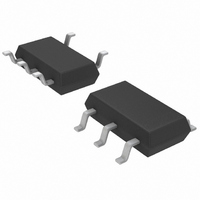
LT1932ES6#TRMPBF Linear Technology, LT1932ES6#TRMPBF Datasheet - Page 4

LT1932ES6#TRMPBF
Manufacturer Part Number
LT1932ES6#TRMPBF
Description
IC LED DRIVR WHITE BCKLGT TSOT-6
Manufacturer
Linear Technology
Type
Backlight, White LEDr
Datasheet
1.LT1932ES6TRMPBF.pdf
(16 pages)
Specifications of LT1932ES6#TRMPBF
Constant Current
Yes
Topology
PWM, Step-Up (Boost)
Number Of Outputs
1
Internal Driver
Yes
Type - Primary
Backlight
Type - Secondary
White LED
Frequency
800kHz ~ 1.6MHz
Voltage - Supply
1 V ~ 10 V
Voltage - Output
36V
Mounting Type
Surface Mount
Package / Case
TSOT-23-6, TSOT-6
Operating Temperature
-40°C ~ 85°C
Current - Output / Channel
40mA
Internal Switch(s)
Yes
Efficiency
80%
Lead Free Status / RoHS Status
Lead free / RoHS Compliant
Other names
LT1932ES6#TRMPBFTR
Available stocks
Company
Part Number
Manufacturer
Quantity
Price
BLOCK DIAGRA
OPERATIO
LT1932
PI FU CTIO S
SW (Pin 1): Switch Pin. This is the collector of the internal
NPN power switch. Minimize the metal trace area con-
nected to this pin to minimize EMI.
GND (Pin 2): Ground Pin. Tie this pin directly to local
ground plane.
LED (Pin 3): LED Pin. This is the collector of the internal
NPN LED switch. Connect the cathode of the bottom LED
to this pin.
The LT1932 uses a constant frequency, current mode
control scheme to regulate the output current, I
Operation can be best understood by referring to the
block diagram in Figure 1. At the start of each oscillator
cycle, the SR latch is set, turning on power switch Q1. The
signal at the noninverting input of the PWM comparator
A2 is proportional to the switch current, summed to-
gether with a portion of the oscillator ramp. When this
signal reaches the level set by the output of error amplifier
A1, comparator A2 resets the latch and turns off the
4
U
U
V
IN
U
U
C1
W
5
SHDN
Q
DRIVER
S
R
6
V
IN
L1
Figure 1. LT1932 Block Diagram
OSCILLATOR
0.04
1.2MHz
2
1
GND
Q1
SW
LED
+
–
5
.
A2
+
–
R
programs the LED current (that flows into the LED pin).
This pin is also used to provide LED dimming.
SHDN (Pin 5): Shutdown Pin. Tie this pin higher than
0.85V to turn on the LT1932; tie below 0.25V to turn it off.
V
capacitor to ground as close to the device as possible.
power switch. In this manner, A1 sets the correct peak
current level to keep the LED current in regulation. If A1’s
output increases, more current is delivered to the output;
if it decreases, less current is delivered. A1 senses the
LED current in switch Q2 and compares it to the current
reference, which is programmed using resistor R
R
I
than 100mV will pull down the output of A1, turning off
power switch Q1 and LED switch Q2.
+
LED
IN
SET
SET
D1
+
, is regulated to 225 • I
(Pin 6): Input Supply Pin. Bypass this pin with a
pin is regulated to 100mV and the output current,
(Pin 4): A resistor between this pin and ground
A1
DRIVER
+
–
I
LED CURRENT
SET
REFERENCE
4
R
R
SET
SET
Q2
SET
3
. Pulling the R
1932 F01
V
OUT
LED
I
LED
C2
SET
pin higher
SET
. The
1932f


