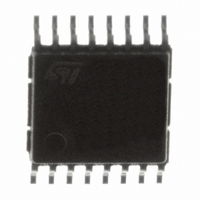
STP08DP05TTR STMicroelectronics, STP08DP05TTR Datasheet - Page 8

STP08DP05TTR
Manufacturer Part Number
STP08DP05TTR
Description
IC LED DRIVER LINEAR 16-TSSOP
Manufacturer
STMicroelectronics
Type
Linear (Serial Interface)r
Datasheet
1.STP08DP05MTR.pdf
(30 pages)
Specifications of STP08DP05TTR
Constant Current
Yes
Topology
8-Bit Shift Register
Number Of Outputs
8
Internal Driver
Yes
Type - Primary
General Purpose
Frequency
30MHz
Voltage - Supply
3 V ~ 5.5 V
Voltage - Output
20V
Mounting Type
Surface Mount
Package / Case
16-TSSOP
Operating Temperature
-40°C ~ 125°C
Current - Output / Channel
100mA
Internal Switch(s)
Yes
Low Level Output Current
- 1 mA
High Level Output Current
1 mA
Operating Supply Voltage
3 V to 3.6 V
Maximum Supply Current
13.5 mA
Maximum Operating Temperature
+ 125 C
Mounting Style
SMD/SMT
Minimum Operating Temperature
- 40 C
Led Driver Application
LED Displays
No. Of Outputs
8
Output Current
100mA
Output Voltage
20V
Input Voltage
3V To 5.5V
For Use With
497-6338 - BOARD EVAL HB 40LED STP08DP05497-6337 - BOARD EVAL HB 40LED STP08DP05
Lead Free Status / RoHS Status
Lead free / RoHS Compliant
Efficiency
-
Lead Free Status / Rohs Status
Details
Other names
497-6029-2
Available stocks
Company
Part Number
Manufacturer
Quantity
Price
Company:
Part Number:
STP08DP05TTR
Manufacturer:
ST
Quantity:
3 000
Part Number:
STP08DP05TTR
Manufacturer:
ST
Quantity:
20 000
Switching characteristics
5
Table 8.
1. In order to achieve high cascade data transfer, please consider tr/tf timings carefully.
8/30
Symbol
t
t
t
t
t
t
t
t
t
PLH1
PLH2
PLH3
PHL1
PHL2
PHL3
t
PLH
PHL
OFF
ON
t
t
r
f
Propagation delay time,
CLK-OUTn, LE\DM1 = H,
OE\DM2 = L
Propagation delay time,
LE\DM1 -OUTn,
OE\DM2 = L
Propagation delay time,
OE\DM2-OUTn,
LE\DM1 = H
Propagation delay time,
CLK-SDO
Propagation delay time,
CLK-OUTn, LE\DM1 = H,
OE\DM2 = L
Propagation delay time,
LE\DM1 -OUTn,
OE\DM2 = L
Propagation delay time,
OE\DM2-OUTn,
LE\DM1 = H
Propagation delay time,
CLK-SDO
Output rise time
10~90% of voltage
waveform
Output fall time
90~10% of voltage
waveform
CLK rise time
CLK fall time
Switching characteristics
Switching characteristics
V
DD
= 5 V, T = 25 °C, unless otherwise specified.
Parameter
(1)
(1)
V
V
I
R
O
DD
IL
EXT
= 20 mA
= GND
= 3.3 V
= 1 KΩ
Doc ID 13405 Rev 4
Test conditions
C
V
R
V
IH
L
L
L
= 10pF
= 3.0 V
= 60 Ω
= V
DD
V
V
V
V
V
V
V
V
V
V
V
V
V
V
V
V
V
V
V
V
DD
DD
DD
DD
DD
DD
DD
DD
DD
DD
DD
DD
DD
DD
DD
DD
DD
DD
DD
DD
= 3.3 V
= 5 V
= 3.3 V
= 5 V
= 3.3 V
= 5 V
= 3.3 V
= 5 V
= 3.3 V
= 5 V
= 3.3 V
= 5 V
= 3.3 V
= 5 V
= 3.3 V
= 5 V
= 3.3 V
= 5 V
= 3.3 V
= 5 V
Min.
Typ.
36
19
38
21
42
23
22
18
25
20
30
15
9
5
4
3
6
3
7
6
STP08DP05
Max.
5000
5000
46.8
24.7
49.4
27.3
28.6
23.4
11.7
32.5
19.5
6.5
5.2
3.9
7.8
3.9
9.1
7.8
54
30
26
39
Unit
ns
ns
ns
ns
ns
ns
ns
ns
ns
ns
ns
ns


