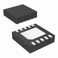
LM2751SD-A/NOPB National Semiconductor, LM2751SD-A/NOPB Datasheet - Page 10

LM2751SD-A/NOPB
Manufacturer Part Number
LM2751SD-A/NOPB
Description
IC LED DRIVR WHITE BCKLGT 10-LLP
Manufacturer
National Semiconductor
Type
Backlight, White LEDr
Datasheet
1.LM2751SD-ANOPB.pdf
(11 pages)
Specifications of LM2751SD-A/NOPB
Topology
PWM, Switched Capacitor (Charge Pump)
Number Of Outputs
1
Internal Driver
Yes
Type - Primary
Backlight
Type - Secondary
White LED
Frequency
725kHz
Voltage - Supply
2.8 V ~ 5.5 V
Voltage - Output
5V
Mounting Type
Surface Mount
Package / Case
10-LLP
Operating Temperature
-40°C ~ 85°C
Current - Output / Channel
80mA
Internal Switch(s)
Yes
Efficiency
90%
Lead Free Status / RoHS Status
Lead free / RoHS Compliant
Other names
LM2751SD-A
LM2751SD-ATR
LM2751SD-ATR
www.national.com
Application Information
The voltage rating of the output capacitor should be 10V or
more. All other capacitors should have a voltage rating at or
above the maximum input voltage of the application.
DRIVING WHITE LEDS
The desired LED current is set by placing a resistor (R) in
series with each LED, and is determined by the equation:
In the equation above, I
a particular LED, and V
at the given current. The output voltage (V
LM2751 is tightly regulated to 4.5V or 5V depending on the
output voltage option. However, LED forward voltage varies
from LED to LED, and LED current will vary accordingly.
Mismatch of LED currents will result in brightness mismatch
from one LED to the next. Therefore it is suggested that LED
groups with tightly controlled I-V characteristics ("Binned"
LEDs) be used. LEDs with looser tolerance can be used in
applications where brightness matching is not critical, such
as in keypad or general backlighting. The typical and maxi-
mum diode forward voltage depends highly on the manufac-
turer and their technology.
PWM BRIGHTNESS CONTROL
Perceived LED brightness can be adjusted using a PWM
control signal on the Enable pin of the LM2751, to turn the
voltage output ON and OFF at a rate faster than perceptible
by the eye. When this is done, the total brightness perceived
is proportional to the duty cycle (D) of the PWM signal (D =
the percentage of time that the LED is on in every PWM
cycle). A simple example: if the LEDs are driven at 15mA
each with a PWM signal that has a 50% duty cycle, per-
ceived LED brightness will be about half as bright as com-
pared to when the LEDs are driven continuously with 15mA.
For linear brightness control over the full duty cycle adjust-
ment range, the PWM frequency (f) should be limited to
accommodate the turn-on time (typ. T
device.
The minimum recommended PWM frequency is 100Hz. Fre-
quencies below this may be visibly noticeable as flicker or
blinking. The maximum recommended PWM frequency is
1kHz. Frequencies above this may cause noise in the au-
dible range.
I
LED
f
MAX
D x (1/f)
= (V
LED
LED
= D
OUT
is the forward voltage of the LED
is the current that flows through
MIN
- V
>
÷ T
T
LED
ON
ON
) ÷R
ON
(Continued)
= 300µs) of the
OUT
) of the
10
THERMAL PROTECTION
When the junction temperature exceeds 150˚C (typ.), inter-
nal thermal protection circuitry disables the device. This
feature protects the LM2751 from damage due to excessive
power dissipation. The device will recover and operate nor-
mally when the junction temperature falls below 140˚C (typ.).
It is important to have good thermal conduction with a proper
layout to reduce thermal resistance.
POWER EFFICIENCY
Charge-Pump efficiency is derived in the following two ideal
equations (supply current and other losses are neglected for
simplicity):
In the equations, G represents the charge pump gain. Effi-
ciency is at its highest as G x V
the efficiency graph in the Typical Performance Character-
istics section for the detailed efficiency data.
POWER DISSIPATION
The power dissipation (P
ture (T
is the product of the input current and input voltage, P
the power consumed by the load connected to the output,
T
ambient thermal resistance for the LLP-10 package. V
the input voltage to the LM2751, V
output of the device, and I
the load connected to V
The junction temperature rating takes precedence over the
ambient temperature rating. The LM2751 may be operated
outside the ambient temperature rating, so long as the junc-
tion temperature of the device does not exceed the maxi-
mum operating rating of 115˚C. The maximum ambient tem-
perature rating must be derated in applications where high
power dissipation and/or poor thermal resistance causes the
junction temperature to exceed 115˚C.
A
is the ambient temperature, and θ
E = (V
J
) can be approximated with the equations below. P
OUT
T
= (V
x I
J
P
= T
OUT
DISSIPATION
IN
A
) ÷ (V
x I
I
+ (P
IN
OUT
IN
DISSIPATION
= G x I
OUT
) − (V
IN
DISSIPATION
.
x I
= P
is the total current supplied to
IN
VOUT
IN
OUT
approaches V
IN
) = V
VOUT
) and junction tempera-
- P
x I
JA
OUT
x θ
OUT
is the voltage at the
OUT
is the junction-to-
JA
÷ (G x V
)
)
OUT
. Refer to
IN
OUT
)
IN
IN
is
is


