LM2753SD/NOPB National Semiconductor, LM2753SD/NOPB Datasheet - Page 9
LM2753SD/NOPB
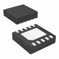
Manufacturer Part Number
LM2753SD/NOPB
Description
IC LED DRIVER PHOTO FLASH 10-LLP
Manufacturer
National Semiconductor
Type
Photo Flash LEDr
Datasheet
1.LM2753SDNOPB.pdf
(12 pages)
Specifications of LM2753SD/NOPB
Topology
PWM, Switched Capacitor (Charge Pump)
Number Of Outputs
1
Internal Driver
Yes
Type - Primary
Flash/Torch
Type - Secondary
White LED
Frequency
725kHz
Voltage - Supply
3 V ~ 5.5 V
Voltage - Output
5V
Mounting Type
Surface Mount
Package / Case
10-LLP
Operating Temperature
-40°C ~ 85°C
Current - Output / Channel
250mA
Internal Switch(s)
Yes
Lead Free Status / RoHS Status
Lead free / RoHS Compliant
Efficiency
-
Other names
LM2753SD
LM2753SDTR
LM2753SDTR


the LM2753 has a switch array with multiple switches con-
nected in parallel.
The number of switches used in parallel depends on the input
voltage applied to the LM2753. At lower input voltages all
paralleled switches are used, and as the input voltage rises,
switches are removed from the parallel configuration. The
highest switch resistance is achieved as the input voltage
reaches the maximum operating voltage, which helps with
voltage management.
THERMAL PROTECTION
When the junction temperature exceeds 140°C (typ.), the
LM2753 internal thermal protection circuitry disables the part.
This feature protects the device from damage due to exces-
sive power dissipation. The device will recover and operate
normally when the junction temperature falls below 125°C
(typ.). It is important to have good thermal conduction with a
proper layout to reduce thermal resistance.
POWER EFFICIENCY
Charge-Pump efficiency is derived in the following two ideal
equations (supply current and other losses are neglected for
simplicity):
In the equations, G represents the charge pump gain. Effi-
ciency is at its highest as G x V
E = (V
OUT
x I
OUT
) ÷ (V
I
IN
= G x I
IN
x I
IN
IN
OUT
approaches V
) = V
OUT
÷ (G x V
OUT
. Refer to
IN
)
9
the efficiency graph in the Typical Performance Character-
istics section for the detailed efficiency data.
POWER DISSIPATION
The power dissipation (P
(T
product of the input current and input voltage, P
power consumed by the load connected to the output, T
the ambient temperature, and θ
thermal resistance for the LLP-10 package. V
voltage to the LM2753, V
the device, and I
connected to both V
The junction temperature rating takes precedence over the
ambient temperature rating. The LM2753 may be operated
outside the ambient temperature rating, so long as the junc-
tion temperature of the device does not exceed the maximum
operating rating of 120°C. The maximum ambient tempera-
ture rating must be derated in applications where high power
dissipation and/or poor thermal resistance causes the junc-
tion temperature to exceed 120°C.
J
) can be approximated with the equations below. P
T
= (V
OUT
J
P
= T
DISSIPATION
OUT
is the total current supplied to the load(s)
IN
A
× I
+ (P
DISSIPATION
and I
IN
VOUT
) − (V
DISSIPATION
OUT
= P
is the voltage at the output of
JA
VOUT
.
IN
) and junction temperature
is the junction-to-ambient
- P
× I
× θ
OUT
OUT
JA
)
)
IN
www.national.com
is the input
OUT
IN
is the
is the
A
is
Related parts for LM2753SD/NOPB
Image
Part Number
Description
Manufacturer
Datasheet
Request
R

Part Number:
Description:
IC,Laser Diode/LED Driver,LLCC,10PIN,PLASTIC
Manufacturer:
National Semiconductor
Part Number:
Description:
National Semiconductor [8-Bit D/A Converter]
Manufacturer:
National Semiconductor
Datasheet:
Part Number:
Description:
National Semiconductor [Media Coprocessor]
Manufacturer:
National Semiconductor
Datasheet:
Part Number:
Description:
Digitally Controlled Tone and Volume Circuit with Stereo Audio Power Amplifier, Microphone Preamp Stage and National 3D Sound
Manufacturer:
National Semiconductor
Datasheet:
Part Number:
Description:
Digitally Controlled Tone and Volume Circuit with Stereo Audio Power Amplifier, Microphone Preamp Stage and National 3D Sound
Manufacturer:
National Semiconductor
Datasheet:
Part Number:
Description:
AC97 Rev 2 Codec with Sample Rate Conversion and National 3D Sound
Manufacturer:
National Semiconductor
Part Number:
Description:
Manufacturer:
National Semiconductor
Datasheet:
Part Number:
Description:
Manufacturer:
National Semiconductor
Datasheet:
Part Number:
Description:
General Purpose, Low Voltage, Low Power, Rail-to-Rail Output Operational Amplifiers
Manufacturer:
National Semiconductor
Datasheet:
Part Number:
Description:
8-bit 20 MSPS flash A/D converter.
Manufacturer:
National Semiconductor
Datasheet:
Part Number:
Description:
Low Noise Quad Operational Amplifier
Manufacturer:
National Semiconductor
Datasheet:
Part Number:
Description:
Quad Differential Line Receivers
Manufacturer:
National Semiconductor
Datasheet:
Part Number:
Description:
Quad High Speed Trapezoidal? Bus Transceiver
Manufacturer:
National Semiconductor
Datasheet:
Part Number:
Description:
Dual Line Receiver
Manufacturer:
National Semiconductor
Datasheet: