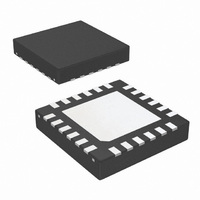
LM27964SQ-C/NOPB National Semiconductor, LM27964SQ-C/NOPB Datasheet - Page 3

LM27964SQ-C/NOPB
Manufacturer Part Number
LM27964SQ-C/NOPB
Description
IC LED DRIVR WHITE BCKLGT 24-LLP
Manufacturer
National Semiconductor
Type
Backlight, White LED (I²C Interface)r
Series
-r
Datasheet
1.LM27964SQ-CNOPB.pdf
(14 pages)
Specifications of LM27964SQ-C/NOPB
Constant Current
Yes
Topology
PWM, Switched Capacitor (Charge Pump)
Number Of Outputs
7
Internal Driver
Yes
Type - Primary
Backlight, General Purpose
Type - Secondary
White LED
Frequency
500kHz ~ 900kHz
Voltage - Supply
2.7 V ~ 5.5 V
Voltage - Output
2 V ~ 4 V
Mounting Type
Surface Mount
Package / Case
24-LLP
Operating Temperature
-30°C ~ 85°C
Current - Output / Channel
30mA
Internal Switch(s)
Yes
Efficiency
87%
Led Driver Application
Camera Phone LED Flash, LED Backlight
No. Of Outputs
7
Output Current
180mA
Input Voltage
2.7V To 5.5V
Operating Temperature Range
-30°C To +85°C
Rohs Compliant
Yes
Constant Voltage
-
Lead Free Status / RoHS Status
Lead free / RoHS Compliant
Other names
LM27964SQ-C
LM27964SQ-C
LM27964SQ-C-TR
LM27964SQ-C
LM27964SQ-C-TR
I
R
V
V
Dxx
Symbol
DxTH
HR
OUT
Absolute Maximum Ratings
If Military/Aerospace specified devices are required,
please contact the National Semiconductor Sales Office/
Distributors for availability and specifications.
Electrical Characteristics
Limits in standard typeface are for T
otherwise specified: V
DKEY = Fullscale Current; ENA, ENB, ENK Bits = “1”; C1=C2=1.0µF, C
and current setting pins (I
V
SCL, SDIO, VIO pin voltages -0.3V to (V
I
Continuous Power Dissipation
(Note 3)
Junction Temperature (T
Storage Temperature Range
Dxx
IN
pin voltage
Pin Voltages
Output Current Regulation
BankA or BankB Enabled
Output Current Regulation
Keypad Driver Enabled
Output Current Regulation
BankA and DKEY Enabled
(Note 10)
Open-Loop Charge Pump Output
Resistance
V
Threshold
Current Source Headroom Voltage
Requirement
(Note 11)
Dxx
1x to 3/2x Gain Transition
IN
Parameter
= 3.6V; V
-0.3V to (V
J-MAX
Dxx
and I
)
DxA
SETx
POUT
J
= 0.4V; V
= 25°C, and limits in boldface type apply over the full operating temperature range. Unless
) apply to BankA, BankB and DKEY. (Note 9)
IN
+0.3V) w/ 6.0V max
+0.3V) w/ 6.0V max
Internally Limited
-65ºC to +150º C
(Notes 2, 8)
-0.3V to 6.0V
DxB
3.0V
BankA or BankB Full-Scale
ENA or ENB = "1", ENK = “0”
3.0V
BankA or BankB Half-Scale
ENA or ENB = "1", ENK = “0”
2.7V
BankA or BankB Full-Scale
ENA or ENB = "1", ENK = “0”
3.0V
DKEY Full-Scale
ENA = ENB = “0”, ENK = “1”
3.2V
R
V
BankA and DKEY Full-Scale
ENA = ENK = “1”, ENB = “0”
Gain = 3/2
Gain = 1
V
I
(I
BankA and/or BankB Full-Scale
Gain = 3/2, ENA and/or ENB = "1"
I
(I
DKEY Full-Scale
Gain = 3/2, ENK = "1"
(Notes 1, 2)
Dxx
DKEY
Dxx
DKEY
SETA
LED
DxA
= 0.4V; V
= 95% ×I
(nom)
and/or V
≤
≤
≤
≤
≤
= 3.6V
= 95% ×I
150ºC
(nom)
= 8.3kΩ, R
V
V
V
V
V
IN
IN
IN
IN
IN
≤
≤
≤
≤
≤
≈
DKEY
≈
Dxx
5.5V
5.5V
3.0V
5.5V
5.5V
15mA)
DxB
DKEY
60mA)
3
(nom.)
SETK
Condition
Falling
= 0.4V; R
(nom.)
Operating Rating
(Notes 1, 2)
Thermal Properties
Maximum Lead Temperature
(Soldering)
ESD Rating (Note 5)
Pins:
Input Voltage Range
LED Voltage Range
Junction Temperature (T
Ambient Temperature (T
(Note 6)
Juntion-to-Ambient Thermal
Resistance (θ
(Note 7)
= 16.9kΩ
IN
Human Body Model - I
Human Body Model - All other
=C
SETA
OUT
=2.2µF; Specifications related to output current(s)
= R
JA
SETB
), SQA24A Package
= R
SETK
A
Dxx
J
) Range
) Range
(-10%)
(-12%)
13.77
52.8
= 16.9kΩ; BankA, BankB, and
Min
Pins:
DKEY
15.3
DxA
2.75
Typ
375
180
180
7.5
15
60
30
60
1
-30°C to +100°C
-30°C to +85°C
(+10%)
(+12%)
16.83
Max
67.2
2.7V to 5.5V
2.0V to 4.0V
www.national.com
41.3°C/W
(Note 4)
1.0kV
2.0kV
Units
mA
(%)
mA
mA
mA
(%)
mA
mV
mV
Ω


