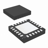
LM3433SQ/NOPB National Semiconductor, LM3433SQ/NOPB Datasheet - Page 4

LM3433SQ/NOPB
Manufacturer Part Number
LM3433SQ/NOPB
Description
IC LED DRIVER HIGH BRIGHT 24-LLP
Manufacturer
National Semiconductor
Series
PowerWise®r
Type
HBLED Driverr
Datasheet
1.LM3433SQNOPB.pdf
(14 pages)
Specifications of LM3433SQ/NOPB
Constant Current
Yes
Topology
PWM, Step-Down (Buck)
Number Of Outputs
1
Internal Driver
No
Type - Primary
Automotive, Backlight
Type - Secondary
High Brightness LED (HBLED)
Frequency
1MHz
Voltage - Supply
3 V ~ 5.8 V
Mounting Type
Surface Mount
Package / Case
24-LLP
Operating Temperature
-40°C ~ 125°C
Internal Switch(s)
No
Efficiency
92%
For Use With
LM3433SQ-36AEV - BOARD EVALUATION FOR LM3433SQ
Lead Free Status / RoHS Status
Lead free / RoHS Compliant
Voltage - Output
-
Current - Output / Channel
-
Other names
LM3433SQTR
www.national.com
SUPPLY CURRENT
I
I
OUTPUT CURRENT CONTROL
V
G
I
I
Gm
ON TIME CONTROL
T
GATE DRIVE AND INTERNAL REGULATOR
V
V
R
R
R
R
IN
IN
CSN
CSP
ONTH
CS
CCOUT
CCILIM
OLH
OHH
OLL
OHL
ADJ
Absolute Maximum Ratings
If Military/Aerospace specified devices are required,
please contact the National Semiconductor Sales Office/
Distributors for availability and specifications.
Electrical Characteristics
Specifications in standard type face are for T
Range ( T
values represent the most likely parametric norm at T
stated the following conditions apply: V
V
V
Symbol
V
COMP, SS to V
BST to HS
V
CGND, DIMR, CSP, CSN,
T
HS to V
LS to V
HO output
DIMO to DIMR
LO output
BST2 to V
Maximum Junction
Temperature
EE
IN
ON
IN
CC
, EN, DIM, ADJ to CGND
to V
to V
EE
EE
EE
EE
J
= −40°C to +125°C). Minimum and Maximum limits are guaranteed through test, design, or statistical correlation. Typical
EE
(Note 2)
V
V
Current sense target voltage;
V
I
(V
Isense Input Current
Isense Input Current
CS to COMP
Transconductance; Gm =
I
16.67)
On time threshold
V
V
HO output low resistance
HO output high resistance
LO output low resistance
LO output high resistance
ADJ
COMP
EE
IN
CS
CC
CC
CNP
Quiescent Current
Quiescent Current
Gain = (V
output regulation w.r.t. V
= V
current limit
EE
-V
/ (V
CSP
CSN
Parameter
CSP
)
– V
– V
ADJ
CSN
-CGND)/
CSN
- V
ADJ
HS-0.3V to BST+0.3V
LS-0.3V to V
EE
/
EE
= -12.0V and V
EN = CGND
EN = V
EN = V
EN = CGND
V
V
w.r.t. CGND
V
V
V
V
V
event
I
V
I = 50mA source
I = 50mA sink
I = 50mA source
I = 50mA sink
CC
-0.3V to +7.5V
-0.3V to +0.3V
-0.3V to 22.0V
J
ADJ
IN
ADJ
ADJ
ADJ
ADJ
T
CC
-0.3V to +16V
-0.3V to +16V
= 25°C and those with boldface type apply over the full Operating Temperature
ON
-0.3V to +7V
-0.3V to +7V
-0.3V to +7V
-0.3V to +7V
= 3.3V, V
= 0mA to 20mA
(Note 1)
= V
- V
= V
= 1V w.r.t. CGND
= V
= V
= 1V w.r.t. CGND
CC
IN
IN
EE
EE
IN
IN
IN
, Not Switching
, Not Switching
150°C
Conditions
+0.3V
J
at terminate ON time
= +25ºC, and are provided for reference purposes only. Unless otherwise
ADJ
IN
= +3.3V with respect to CGND.
= 0.5V or 1.5V
4
Operating Conditions
Power Dissipation(Note 3)
ESD Susceptibility
(Note 4)
Operating Junction
Temperature Range (Note 5)
Storage Temperature
Input Voltage V
Input Voltage V
ADJ Input Voltage Range to
CGND
CSP, CSN Common Mode
Range With Respect to CGND
Human Body Model
Machine Model
Charge Device Model
Min(Note 5) Typ(Note 6) Max(Note 5)
230
0.6
6.3
57
15
33
IN
EE
w.r.t. CGND
w.r.t. CGND
16.67
6.75
300
287
1.0
-50
1.3
35
60
10
60
53
3
1
2
3
2
3
334
2.2
7.1
19
71
63
18
Internally Limited
−40°C to +125°C
−65°C to +150°C
3.0V to 5.8V
-9V to -14V
-6V to 0V
0V to V
Units
200V
V/V
mA
mV
mS
mV
mA
µA
µA
µA
µA
Ω
Ω
V
2kV
1kV
IN


