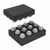
LM3530UME-40/NOPB National Semiconductor, LM3530UME-40/NOPB Datasheet - Page 38

LM3530UME-40/NOPB
Manufacturer Part Number
LM3530UME-40/NOPB
Description
IC LED DRVR PROGRAM I2C 12USMD
Manufacturer
National Semiconductor
Series
PowerWise®r
Datasheet
1.LM3530UME-40NOPB.pdf
(44 pages)
Specifications of LM3530UME-40/NOPB
Topology
PWM, Step-Up (Boost)
Number Of Outputs
1
Internal Driver
Yes
Type - Primary
Backlight
Type - Secondary
White LED
Frequency
500kHz
Voltage - Supply
2.7 V ~ 5.5 V
Mounting Type
Surface Mount
Package / Case
12-UFBGA
Operating Temperature
-40°C ~ 85°C
Current - Output / Channel
Adjustable
Led Driver Application
LED Backlighting, Portable Electronics
No. Of Outputs
1
Output Current
29.5mA
Output Voltage
40V
Input Voltage
2.7V To 5.5V
Rohs Compliant
Yes
Lead Free Status / RoHS Status
Lead free / RoHS Compliant
Voltage - Output
-
Other names
LM3530UME-40TR
www.national.com
Schottky Diode Placement
The Schottky diode is in the path of the inductor current dis-
charge. As a result the Schottky diode sees a high current
step from 0 to I
diode turns on. Any inductance in series with the diode will
cause a voltage spike (V
which can potentially over-voltage the SW pin, or feed through
to V
necting the anode of the diode as close as possible to the SW
pin and the cathode of the diode as close as possible to C
+ will reduce the inductance (L
spikes (see
Inductor Placement
The node where the inductor connects to the LM3530’s SW
bump has 2 issues. First, a large switched voltage (0 to
V
cycle. This switched voltage can be capacitively coupled into
nearby nodes. Second, there is a relatively large current (in-
put current) on the traces connecting the input supply to the
inductor and connecting the inductor to the SW bump. Any
resistance in this path can cause large voltage drops that will
negatively affect efficiency.
To reduce the capacitively coupled signal from SW into near-
by traces, the SW bump to inductor connection must be
minimized in area. This limits the PCB capacitance from SW
to other traces. Additionally, the other traces need to be rout-
ed away from SW and not directly beneath. This is especially
true for high impedance nodes that are more susceptible to
capacitive coupling such as (SCL, SDA, HWEN, PWM, and
possibly ASL1 and ALS2). A GND plane placed directly below
SW will dramatically reduce the capacitance from SW into
nearby traces
To limit the trace resistance of the VBATT to inductor con-
nection and from the inductor to SW connection, use short,
wide traces (see
Input Capacitor Selection and Placement
The input bypass capacitor filters the inductor current ripple,
and the internal MOSFET driver currents during turn on of the
power switch.
The driver current requirement can range from 50mA at 2.7V
to over 200mA at 5.5V with fast durations of approximately
10ns to 20ns. This will appear as high di/dt current pulses
OUT
OUT
+ V
and through the output capacitor and into GND. Con-
F_SCHOTTKY
Figure
PEAK
Figure
28,
) appears on this node every switching
each time the switch turns off and the
Figure 29
28,
SPIKE
Figure 29
P_
= L
) and minimize these voltage
,
P_
andFigure 30
× dI/dt) at SW and OUT
, and
Figure
).
30).
OUT
38
coming from the input capacitor each time the switch turns on.
Close placement of the input capacitor to the IN pin and to the
GND pin is critical since any series inductance between IN
and C
could appear on the V
Close placement of the input bypass capacitor at the input
side of the inductor is also critical. The source impedance (in-
ductance and resistance) from the input supply, along with the
input capacitor of the LM3530, form a series RLC circuit. If the
output resistance from the source (R
cuit will be underdamped and will have a resonant frequency
(typically the case). Depending on the size of L
frequency could occur below, close to, or above the LM3530's
switching frequency. This can cause the supply current ripple
to be:
1.
2.
3.
Equation 1is the criteria for an underdamped response. Equa-
tion 2 is the resonant frequency. Equation 3 is the approxi-
mated supply current ripple as a function of L
As an example, consider a 3.6V supply with 0.1Ω of series
resistance connected to C
traces. This results in an underdamped input filter circuit with
a resonant frequency of 712kHz. Since the switching fre-
quency lies near to the resonant frequency of the input RLC
network, the supply current is probably larger then the induc-
tor current ripple. In this case using equation 3 from
27
the inductor current ripple. Increasing the series inductance
(L
around 225kHz and the supple current ripple to be approxi-
mately 0.25×'s the inductor current ripple.
S
the supply current ripple can be approximated as 1.68×'s
) to 500nH causes the resonant frequency to move to
Approximately equal to the inductor current ripple when
the resonant frequency occurs well above the LM3530's
switching frequency;
Greater then the inductor current ripple when the
resonant frequency occurs near the switching frequency;
and
Less then the inductor current ripple when the resonant
frequency occurs well below the switching frequency.
Figure 27
output impedance of the supply and the input capacitor.
The circuit is re-drawn for the AC case where the V
supply is replaced with a short to GND and the LM3530
+ Inductor is replaced with a current source (ΔI
IN
+ or C
shows the series RLC circuit formed from the
IN
- and GND can create voltage spikes that
IN
supply line and in the GND plane.
IN
through 50nH of connecting
S
) is low enough the cir-
S
S
, R
the resonant
S
, and C
L
).
Figure
IN
IN
.


