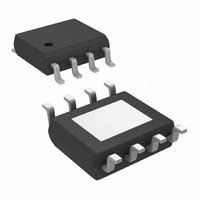
LM3402HVMR/NOPB National Semiconductor, LM3402HVMR/NOPB Datasheet - Page 25

LM3402HVMR/NOPB
Manufacturer Part Number
LM3402HVMR/NOPB
Description
IC LED DRVR HP CONST CURR 8-PSOP
Manufacturer
National Semiconductor
Series
PowerWise®r
Type
High Power, Constant Currentr
Specifications of LM3402HVMR/NOPB
Constant Current
Yes
Topology
PWM, Step-Down (Buck)
Number Of Outputs
1
Internal Driver
Yes
Type - Primary
Automotive
Type - Secondary
High Brightness LED (HBLED), White LED
Frequency
1MHz
Voltage - Supply
6 V ~ 75 V
Mounting Type
Surface Mount
Package / Case
8-PSOP
Operating Temperature
-40°C ~ 125°C
Current - Output / Channel
500mA
Internal Switch(s)
Yes
Efficiency
96%
Primary Input Voltage
75V
No. Of Outputs
1
Output Voltage
73V
Output Current
500mA
Voltage Regulator Case Style
PSOP
No. Of Pins
8
Operating Temperature Range
-40°C To +125°C
Svhc
No SVHC (15-Dec-2010)
Rohs Compliant
Yes
For Use With
551600000-001A/NOPB - BOARD WEBENCH SO8/SOP LM3404/2551600003-001A - BOARD WEBENCH MSOP LM3402LM3402HVEVAL - BOARD EVALUATION FOR LM3402HV
Lead Free Status / RoHS Status
Lead free / RoHS Compliant
Voltage - Output
-
Other names
LM3402HVMR
Available stocks
Company
Part Number
Manufacturer
Quantity
Price
Part Number:
LM3402HVMR/NOPB
Manufacturer:
NS/国半
Quantity:
20 000
DCR loss, P
Recirculating diode loss, P
Current Sense Resistor Loss, P
Electrical efficiency, η = P
17.76 / (17.76 + 0.62) = 96%
Temperature Rise in the LM3402HV IC is calculated as:
Layout Considerations
The performance of any switching converter depends as
much upon the layout of the PCB as the component selection.
The dark grey, inner loop represents the high current path
during the MOSFET on-time. The light grey, outer loop rep-
resents the high current path during the off-time.
GROUND PLANE AND SHAPE ROUTING
The diagram of Figure 6 is also useful for analyzing the flow
of continuous current vs. the flow of pulsating currents. The
circuit paths with current flow during both the on-time and off-
time are considered to be continuous current, while those that
carry current during the on-time or off-time only are pulsating
currents. Preference in routing should be given to the pulsat-
ing current paths, as these are the portions of the circuit most
likely to emit EMI. The ground plane of a PCB is a conductor
and return path, and it is susceptible to noise injection just as
any other circuit path. The continuous current paths on the
ground net can be routed on the system ground plane with
less risk of injecting noise into other circuits. The path be-
tween the input source and the input capacitor and the path
between the recirculating diode and the LEDs/current sense
resistor are examples of continuous current paths. In contrast,
the path between the recirculating diode and the input capac-
itor carries a large pulsating current. This path should be
routed with a short, thick shape, preferably on the component
side of the PCB. Multiple vias in parallel should be used right
T
LM3402
= (P
P
L
C
L
, in the inductor
= I
+ P
F
2
G
x DCR = 0.35
+ P
S
) x θ
= 74.8°C
O
D
/ (P
JA
= 42 mW
= (0.16 + 0.084 + 0.13) x 200
SNS
O
2
x 1.1 = 135 mW
+ Sum of all loss terms) =
= 69 mW
FIGURE 13. Buck Converter Current Loops
25
The following guidelines will help the user design a circuit with
maximum rejection of outside EMI and minimum generation
of unwanted EMI.
COMPACT LAYOUT
Parasitic inductance can be reduced by keeping the power
path components close together and keeping the area of the
loops that high currents travel small. Short, thick traces or
copper pours (shapes) are best. In particular, the switch node
(where L1, D1, and the SW pin connect) should be just large
enough to connect all three components without excessive
heating from the current it carries. The LM3402/02HV oper-
ates in two distinct cycles whose high current paths are shown
in Figure 6:
at the pad of the input capacitor to connect the component
side shapes to the ground plane. A second pulsating current
loop that is often ignored is the gate drive loop formed by the
SW and BOOT pins and capacitor CB. To minimize this loop
at the EMI it generates, keep CB close to the SW and BOOT
pins.
CURRENT SENSING
The CS pin is a high-impedance input, and the loop created
by R
as small as possible to maximize noise rejection. R
therefore be placed as close as possible to the CS and GND
pins of the IC.
REMOTE LED ARRAYS
In some applications the LED or LED array can be far away
(several inches or more) from the LM3402/02HV, or on a sep-
arate PCB connected by a wiring harness. When an output
capacitor is used and the LED array is large or separated from
the rest of the converter, the output capacitor should be
placed close to the LEDs to reduce the effects of parasitic
inductance on the AC impedance of the capacitor. The current
sense resistor should remain on the same PCB, close to the
LM3402/02HV.
SNS
, R
Z
(if used), the CS pin and ground should be made
20192128
www.national.com
SNS
should


