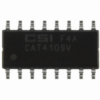
CAT4109V-GT2 ON Semiconductor, CAT4109V-GT2 Datasheet - Page 9

CAT4109V-GT2
Manufacturer Part Number
CAT4109V-GT2
Description
IC LED DRIVER RGB 16-SOIC
Manufacturer
ON Semiconductor
Type
RGB LED Driverr
Datasheet
1.CAT4109V-GT2.pdf
(12 pages)
Specifications of CAT4109V-GT2
Constant Current
Yes
Topology
PWM
Number Of Outputs
3
Internal Driver
Yes
Type - Primary
Backlight
Type - Secondary
RGB
Voltage - Supply
3 V ~ 5.5 V
Voltage - Output
25V
Mounting Type
Surface Mount
Package / Case
16-SOIC (3.9mm Width)
Operating Temperature
-40°C ~ 85°C
Current - Output / Channel
175mA
Internal Switch(s)
No
Operating Supply Voltage (typ)
3.3/5V
Operating Temperature (min)
-40C
Operating Temperature (max)
85C
Operating Temperature Classification
Industrial
Package Type
SOIC
Pin Count
16
Mounting
Surface Mount
Operating Supply Voltage (min)
3V
Operating Supply Voltage (max)
5.5V
Number Of Digits
3
Low Level Output Current
175 mA
High Level Output Current
200 mA
Operating Supply Voltage
3 V to 5.5 V
Maximum Supply Current
10 mA
Maximum Operating Temperature
+ 85 C
Mounting Style
SMD/SMT
Minimum Operating Temperature
- 40 C
Lead Free Status / RoHS Status
Lead free / RoHS Compliant
Frequency
-
Efficiency
-
Lead Free Status / Rohs Status
Compliant
Other names
CAT4109V-GT2TR
Application Information
Power Dissipation
calculated as follows:
where V
associated LED current. Combinations of high V
voltage or high ambient temperature can cause the CAT4109
to enter thermal shutdown. In applications where V
high, a resistor can be inserted in series with the LED string
to lower P
primarily of two paths in series. The first path is the junction
to the case (q
package style, and the second path is the case to ambient
(q
layout. The overall junction to ambient (q
resistance is equal to:
junction temperature T
dissipation P
following equation:
with two square inches of copper allocated for “heat
spreading”, the resulting q
power dissipation is calculated as follow:
The power dissipation (P
Thermal dissipation of the junction heat consists
CA
For a given package style and board layout, the operating
When mounted on a double−sided printed circuit board
For example, at 60°C ambient temperature, the maximum
P
) thermal resistance, which is dependent on board
T
Dmax
J
+ T
LEDN
P
D
D
+
.
AMB
D
+ V
JC
, and the ambient temperature, resulting in the
is the voltage at the LED pin, and I
(T
) thermal resistance which is defined by the
) P
Jmax
DD
q
q
D
* T
JA
JA
(q
I
DD
+ q
JC
J
AMB
JA
is a function of the power
) q
) S V
JC
is about 74°C/W.
)
D
+
) of the CAT4109 can be
) q
CA
(150 * 60)
) + T
LEDN
CA
74
AMB
I
LEDN
) P
+ 1.2 W
JA
LEDN
D
) thermal
q
LEDN
JA
http://onsemi.com
is the
LED
is
9
Recommended Layout
possible. RSET resistors should be directly connected to the
GND pin of the device. For better thermal dissipation,
multiple via can be used to connect the GND pad to a large
ground plane. It is also recommended to use large pads and
traces on the PCB wherever possible to spread out the heat.
The LEDs for this layout are driven from a separate supply
(VLED+), but they can also be driven from the same supply
connected to VDD.
Bypass capacitor C1 should be placed as close to the IC as
Figure 15. Recommended Layout


