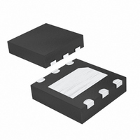
MAX16820ATT+T Maxim Integrated Products, MAX16820ATT+T Datasheet - Page 2

MAX16820ATT+T
Manufacturer Part Number
MAX16820ATT+T
Description
IC LED DRIVER HIGH BRIGHT 6-TDFN
Manufacturer
Maxim Integrated Products
Type
HBLED Driverr
Datasheet
1.MAX16820ATTT.pdf
(10 pages)
Specifications of MAX16820ATT+T
Constant Current
Yes
Topology
PWM, Step-Down (Buck)
Number Of Outputs
1
Internal Driver
No
Type - Primary
Automotive
Type - Secondary
*
Frequency
2MHz
Voltage - Supply
4.5 V ~ 28 V
Voltage - Output
4 V ~ 5.5 V
Mounting Type
Surface Mount
Package / Case
6-TDFN Exposed Pad
Operating Temperature
-40°C ~ 125°C
Current - Output / Channel
1A
Internal Switch(s)
No
Low Level Output Current
1000000 uA (Typ)
High Level Output Current
50000 uA (Typ)
Operating Supply Voltage
4.5 V to 28 V
Maximum Supply Current
425 uA
Maximum Power Dissipation
1454 mW
Maximum Operating Temperature
+ 125 C
Mounting Style
SMD/SMT
Minimum Operating Temperature
- 40 C
Lead Free Status / RoHS Status
Lead free / RoHS Compliant
Efficiency
-
Lead Free Status / Rohs Status
Lead free / RoHS Compliant
Other names
MAX16820ATT+T
MAX16820ATT+TTR
MAX16820ATT+TTR
ABSOLUTE MAXIMUM RATINGS
IN, CSN, DIM to GND .............................................-0.3V to +30V
V
CSN to IN...............................................................-0.3V to +0.3V
Maximum Current into Any Pin
Continuous Power Dissipation (T
2MHz High-Brightness LED Drivers with
High-Side Current Sense and 5000:1 Dimming
Stresses beyond those listed under “Absolute Maximum Ratings” may cause permanent damage to the device. These are stress ratings only, and functional
operation of the device at these or any other conditions beyond those indicated in the operational sections of the specifications is not implied. Exposure to
absolute maximum rating conditions for extended periods may affect device reliability.
ELECTRICAL CHARACTERISTICS
(V
T
2
Input Voltage Range
Maximum Current Regulator
Switching Frequency
Ground Current
Supply Current
Undervoltage Lockout
Undervoltage Lockout Hysteresis
SENSE COMPARATOR
Sense Voltage Threshold High
Sense Voltage Threshold Low
Propagation Delay to Output
High
Propagation Delay to Output Low
Current-Sense Input Current
Current-Sense Threshold
Hysteresis
CC
A
(except IN, V
IN
6-Pin TDFN (derate 18.17mW/
= +25°C.) (Note 1)
, DRV to GND ....................................................-0.3V to +6V
_______________________________________________________________________________________
= 12V, V
PARAMETER
DIM
CC
, and DRV)............................................±20mA
= V
IN
, C
VCC
= 1µF, R
A
o
C
= +70°C)
*
above +70°C).......1454mW
SYMBOL
V
V
CS
UVLO
t
t
I
SNSLO
DPDH
I
SNSHI
DPDL
f
GND
V
CSN
SW
I
SENSE
IN
HYS
IN
= 0.5Ω, T
DRV open
V
V
V
V
V
(V
0.5V (MAX16820)
(V
0.5V (MAX16819)
(V
(V
(V
(V
Falling edge of (V
0V to DRV high, C
Rising edge of (V
0.26V to DRV low, C
(V
MAX16819
MAX16820
DIM
IN
DRV
IN
DRV
IN
IN
IN
CC
IN
CC
IN
= V
= V
- V
- V
- V
- V
- V
- 0.5V) (MAX16820)
- 0.5V) (MAX16819)
< 0.6V
> V
< 0.5V
CSN
CSN
CSN
CSN
CSN
CSN
CSN
A
CC
= T
) rising from 0V until V
) rising from 0V until V
) falling from 0.26V until V
) falling from 0.26V until V
) = 200mV
= V
= V
- 0.5V
J
CONDITIONS
DIM
DIM
= -40°C to +125°C, unless otherwise noted. Typical values are at
IN
IN
DRV
, V
, V
Operating Temperature Range .........................-40°C to +125°C
Junction Temperature ......................................................+150°C
Storage Temperature Range .............................-65°C to +150°C
Lead Temperature (soldering, 10s) .................................+300°C
Pin-to-Pin ESD Ratings (HB Model).....................................2.5kV
*As per JEDEC51 Standard (Single-Layer Board).
- V
- V
DRV
IN
IN
= 1nF
CSN
CSN
rising from 4V until
falling from 6V,
= 1nF
) from 0V to
) from 0.26V to
DRV
DRV
DRV
DRV
<
<
>
>
MIN
195
213
176
158
4.5
TYP
210
230
190
170
4.7
0.5
82
82
56
17
MAX
28.0
425
225
246
204
182
1.5
5.0
4.5
70
35
2
1
UNITS
MHz
mA
mV
mV
mV
mV
µA
µA
ns
ns
V
V
V


