LP3943ISQ/NOPB National Semiconductor, LP3943ISQ/NOPB Datasheet - Page 4
LP3943ISQ/NOPB
Manufacturer Part Number
LP3943ISQ/NOPB
Description
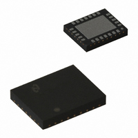
IC LED DRIVER RGB 24-LLP
Manufacturer
National Semiconductor
Series
PowerWise®r
Type
RGB LED Driverr
Datasheet
1.LP3943ISQNOPB.pdf
(13 pages)
Specifications of LP3943ISQ/NOPB
Topology
PWM, Step-Up (Boost)
Number Of Outputs
16
Internal Driver
Yes
Type - Primary
LED Blinker, Light Management Unit (LMU)
Type - Secondary
RGB, White LED
Frequency
400kHz
Voltage - Supply
2.3 V ~ 5.5 V
Mounting Type
Surface Mount
Package / Case
24-LLP
Operating Temperature
-40°C ~ 85°C
Current - Output / Channel
25mA
Internal Switch(s)
Yes
For Use With
LP3943ISQEV - BOARD EVAL FOR LP3943 FUNLIGHT
Lead Free Status / RoHS Status
Lead free / RoHS Compliant
Voltage - Output
-
Efficiency
-
Other names
LP3943ISQ
LP3943ISQTR
LP3943ISQTR
Available stocks
Company
Part Number
Manufacturer
Quantity
Price
Company:

Part Number:
LP3943ISQ/NOPB
Manufacturer:
TI
Quantity:
8 102
Part Number:
LP3943ISQ/NOPB
Manufacturer:
TI/德州仪器
Quantity:
20 000


www.national.com
POWER SUPPLY
V
I
∆I
V
t
LED
V
V
I
I
C
ALL DIGITAL PINS (EXCEPT SCL AND SDA PINS)
V
V
I
C
I
V
V
V
I
F
t
t
Q
w
OL
LEAK
LEAK
2
OL
HOLD
CLK-LP
Symbol
CLK
Absolute Maximum Ratings
1)
If Military/Aerospace specified devices are required,
please contact the National Semiconductor Sales Office/
Distributors for availability and specifications.
Electrical Characteristics
Unless otherwise noted, V
in boldface type apply over the entire junction temperature range for operation, T
DD
POR
IL
IH
IL
IH
IL
IH
OL
I/O
IN
C INTERFACE (SCL AND SDA PINS)
Q
V
A0, A1, A2, SCL, SDA, RST
Voltage on LED pins
Junction Temperature
Storage Temperature
Power Dissipation (Note 3)
DD
(Collectively called digital pins)
Supply Voltage
Supply Current
Additional Standby Current
Power-On Reset Voltage
Reset Pulse Width
LOW Level Input Voltage
HIGH Level Input Voltage
Low Level Output Current
(Note 6)
Input Leakage Current
Input/Output Capacitance
LOW Level Input Voltage
HIGH Level Input Voltage
Input Leakage Current
Input Capacitance
LOW Level Input Voltage
HIGH Level Input Voltage
LOW Level Output Voltage
LOW Level Output Current
Clock Frequency
Hold Time Repeated START
Condition
CLK Low Period
Parameter
DD
= 5.5V. Typical values and limits appearing in normal type apply for T
V
−65˚C to 150˚C
No Load
Standby
V
at 4.3V
V
V
V
V
V
V
V
(Note 7)
V
V
(Note 7)
(Note 7)
(Note 7)
SS
DD
OL
OL
OL
OL
OL
OL
DD
IN
OL
(Notes 2,
−0.5V to 6V
−0.5V to 6V
= 0V (Note 7)
= 0.4V, V
= 0.4V, V
= 0.4V, V
= 0.7V, V
= 0.7V, V
= 0.7V, V
= 0.4V
= 5.5V, every LED pin
= 3.6, V
400 mW
Conditions
150˚C
IN
6V
DD
DD
DD
DD
DD
DD
= 0V or V
= 2.3V
= 3.0V
= 5.0V
= 2.3V
= 3.0V
= 5.0V
4
Operating Ratings
ESD (Note 4)
V
Junction Temperature
Operating Ambient Temperature
Thermal Resistance (θ
DD
DD
Human Body Model
Machine Model
Charge Device Model
LLP24 (Note 3)
Typical
350
2.0
1.8
2.6
2.3
6.5
10
J
5
= −40˚C to +125˚C. (Note 5)
JA
)
0.7V
−0.5
−0.5
Min
-0.5
2.3
2.0
2.0
0.6
1.3
−1
−1
12
15
15
20
25
9
0
3
DD
(Notes 1, 2)
J
Limit
= 25˚C. Limits appearing
Max
0.3V
0.2V
1.96
550
400
5.5
0.8
5.5
0.8
5.5
5.5
5
2
1
5
1
5
−40˚C to +125˚C
−40˚C to +85˚C
DD
DD
2.3V to 5.5V
37˚C/W
Units
kHz
200V
mA
mA
mA
µA
µA
pF
µA
pF
ns
µs
µs
2 kV
1 kV
V
V
V
V
V
V
V
V
V
Related parts for LP3943ISQ/NOPB
Image
Part Number
Description
Manufacturer
Datasheet
Request
R

Part Number:
Description:
LED Driver IC
Manufacturer:
National Semiconductor
Datasheet:

Part Number:
Description:
National Semiconductor [8-Bit D/A Converter]
Manufacturer:
National Semiconductor
Datasheet:
Part Number:
Description:
National Semiconductor [Media Coprocessor]
Manufacturer:
National Semiconductor
Datasheet:
Part Number:
Description:
Digitally Controlled Tone and Volume Circuit with Stereo Audio Power Amplifier, Microphone Preamp Stage and National 3D Sound
Manufacturer:
National Semiconductor
Datasheet:
Part Number:
Description:
Digitally Controlled Tone and Volume Circuit with Stereo Audio Power Amplifier, Microphone Preamp Stage and National 3D Sound
Manufacturer:
National Semiconductor
Datasheet:
Part Number:
Description:
AC97 Rev 2 Codec with Sample Rate Conversion and National 3D Sound
Manufacturer:
National Semiconductor
Part Number:
Description:
Manufacturer:
National Semiconductor
Datasheet:
Part Number:
Description:
Manufacturer:
National Semiconductor
Datasheet:
Part Number:
Description:
General Purpose, Low Voltage, Low Power, Rail-to-Rail Output Operational Amplifiers
Manufacturer:
National Semiconductor
Datasheet:
Part Number:
Description:
8-bit 20 MSPS flash A/D converter.
Manufacturer:
National Semiconductor
Datasheet:
Part Number:
Description:
Low Noise Quad Operational Amplifier
Manufacturer:
National Semiconductor
Datasheet:
Part Number:
Description:
Quad Differential Line Receivers
Manufacturer:
National Semiconductor
Datasheet:
Part Number:
Description:
Quad High Speed Trapezoidal? Bus Transceiver
Manufacturer:
National Semiconductor
Datasheet: