LM27964SQ-I National Semiconductor, LM27964SQ-I Datasheet - Page 8
LM27964SQ-I
Manufacturer Part Number
LM27964SQ-I
Description
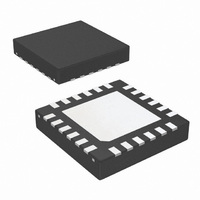
IC LED DRIVR WHITE BCKLGT 24-LLP
Manufacturer
National Semiconductor
Type
Backlight, White LED (I²C Interface)r
Datasheet
1.LM27964SQ-CNOPB.pdf
(14 pages)
Specifications of LM27964SQ-I
Constant Current
Yes
Topology
PWM, Switched Capacitor (Charge Pump)
Number Of Outputs
7
Internal Driver
Yes
Type - Primary
Backlight, General Purpose
Type - Secondary
White LED
Frequency
500kHz ~ 900kHz
Voltage - Supply
2.7 V ~ 5.5 V
Voltage - Output
2 V ~ 4 V
Mounting Type
Surface Mount
Package / Case
24-LLP
Operating Temperature
-30°C ~ 85°C
Current - Output / Channel
30mA
Internal Switch(s)
Yes
Efficiency
87%
Lead Free Status / RoHS Status
Contains lead / RoHS non-compliant
Other names
LM27964SQ-ITR
Available stocks
Company
Part Number
Manufacturer
Quantity
Price
Company:

Part Number:
LM27964SQ-I/NOPB
Manufacturer:
NS
Quantity:
925


www.national.com
Circuit Description
OVERVIEW
The LM27964 is a white LED driver system based upon an
adaptive 1.5×/1× CMOS charge pump capable of supplying
up to 180mA of total output current. With three separately
controlled banks of constant current sinks, the LM27964 is an
ideal solution for platforms requiring a single white LED driver
for main and sub displays, as well as other general purpose
lighting needs. The tightly matched current sinks ensure uni-
form brightness from the LEDs across the entire small-format
display.
Each LED is configured in a common anode configuration,
with the peak drive current being programmed through the
use of external R
used to enable and vary the brightness within the individual
current sink banks. For BankA and BankB, 16 levels of PWM
brightness control are available, while 4 analog levels are
present for the DKEY driver.
CIRCUIT COMPONENTS
Charge Pump
The input to the 1.5x/1x charge pump is connected to the
V
nected to the V
range of the LM27964 is 3.0V to 5.5V. The device’s regulated
charge pump has both open loop and closed loop modes of
operation. When the device is in open loop, the voltage at
V
the device is in closed loop, the voltage at V
to 4.6V (typ.). The charge pump gain transitions are actively
selected to maintain regulation based on LED forward voltage
and load requirements. This allows the charge pump to stay
in the most efficient gain (1x) over as much of the input voltage
range as possible, reducing the power consumed from the
battery.
LED Forward Voltage Monitoring
The LM27964 has the ability to switch converter gains (1x or
3/2x) based on the forward voltage of the LED load. This abil-
ity to switch gains maximizes efficiency for a given load.
Forward voltage monitoring occurs on all diode pins within
BankA and BankB (DKEY is not monitored). At higher input
voltages, the LM27964 will operate in pass mode, allowing
the POUT voltage to track the input voltage. As the input volt-
age drops, the voltage on the DXX pins will also drop (V
= V
voltage approximately equal to 375mV, the charge pump will
then switch to the gain of 3/2. This switchover ensures that
the current through the LEDs never becomes pinched off due
to a lack of headroom on the current sources.
Only active Dxx pins will be monitored. For example, if only
BankA is enabled, the LEDs in BankB will not affect the gain
transition point. If both banks are enabled, all diodes will be
monitored, and the gain transition will be based upon the
diode with the highest forward voltage. The DKEY pin is not
monitored as it is intended to be for keypad LEDs. Keypad
LEDs generally require lower current, resulting in lower for-
ward voltage compared to the BankA and BankB LEDs that
have higher currents. In the event that only the DKEY driver
is enabled without either BankA or BankB, the charge pump
will default to 3/2 mode to ensure the DKEY driver has enough
headroom.
It is not recommended that any of the BankA or BankB drivers
be left disconnected if either bank will be used in the applica-
IN
OUT
POUT
pin, and the regulated output of the charge pump is con-
is equal to the gain times the voltage at the input. When
– V
LEDx
). Once any of the active Dxx pins reaches a
SETx
OUT
resistors. An I
pin. The recommended input voltage
2
C compatible interface is
OUT
is regulated
DXX
8
tion. If Dxx pin/s are left unconnected, the LM27964 will
default to the gain of 3/2. If the BankA or BankB drivers are
not going to be used in the application, leaving the Dxx pins
is acceptable as long as the ENx bit in the general purpose
register is set to "0".
I
DATA VALIDITY
The data on SDIO line must be stable during the HIGH period
of the clock signal (SCL). In other words, state of the data line
can only be changed when CLK is LOW.
A pull-up resistor between VIO and SDIO must be greater
than [ (VIO-V
Using a larger pull-up resistor results in lower switching cur-
rent with slower edges, while using a smaller pull-up results
in higher switching currents with faster edges.
START AND STOP CONDITIONS
START and STOP conditions classify the beginning and the
end of the I
signal transitioning from HIGH to LOW while SCL line is
HIGH. A STOP condition is defined as the SDIO transitioning
from LOW to HIGH while SCL is HIGH. The I
generates START and STOP conditions. The I
sidered to be busy after a START condition and free after a
STOP condition. During data transmission, the I
can generate repeated START conditions. First START and
repeated START conditions are equivalent, function-wise.
The data on SDIO line must be stable during the HIGH period
of the clock signal (SCL). In other words, the state of the data
line can only be changed when CLK is LOW.
TRANSFERING DATA
Every byte put on the SDIO line must be eight bits long, with
the most significant bit (MSB) being transferred first. Each
byte of data has to be followed by an acknowledge bit. The
acknowledge related clock pulse is generated by the master.
The master releases the SDIO line (HIGH) during the ac-
knowledge clock pulse. The LM27964 pulls down the SDIO
line during the 9th clock pulse, signifying an acknowledge.
The LM27964 generates an acknowledge after each byte has
been received.
2
C Compatible Interface
FIGURE 2. Start and Stop Conditions
2
C session. A START condition is defined as SDIO
FIGURE 1. Data Validity Diagram
OL
) / 2mA] to meet the V
OL
requirement on SDIO.
2
C master always
2
C bus is con-
2
C master
20138106
20138111
Related parts for LM27964SQ-I
Image
Part Number
Description
Manufacturer
Datasheet
Request
R

Part Number:
Description:
Accurate, 120 C-150 C Factory Preset Thermostat Lm27 Form
Manufacturer:
National Semiconductor Corporation
Datasheet:

Part Number:
Description:
Factory Preset Thermostat
Manufacturer:
National Semiconductor
Datasheet:
Part Number:
Description:
National Semiconductor [8-Bit D/A Converter]
Manufacturer:
National Semiconductor
Datasheet:
Part Number:
Description:
National Semiconductor [Media Coprocessor]
Manufacturer:
National Semiconductor
Datasheet:
Part Number:
Description:
Digitally Controlled Tone and Volume Circuit with Stereo Audio Power Amplifier, Microphone Preamp Stage and National 3D Sound
Manufacturer:
National Semiconductor
Datasheet:
Part Number:
Description:
Digitally Controlled Tone and Volume Circuit with Stereo Audio Power Amplifier, Microphone Preamp Stage and National 3D Sound
Manufacturer:
National Semiconductor
Datasheet:
Part Number:
Description:
AC97 Rev 2 Codec with Sample Rate Conversion and National 3D Sound
Manufacturer:
National Semiconductor
Part Number:
Description:
Manufacturer:
National Semiconductor
Datasheet:
Part Number:
Description:
Manufacturer:
National Semiconductor
Datasheet:
Part Number:
Description:
General Purpose, Low Voltage, Low Power, Rail-to-Rail Output Operational Amplifiers
Manufacturer:
National Semiconductor
Datasheet:
Part Number:
Description:
8-bit 20 MSPS flash A/D converter.
Manufacturer:
National Semiconductor
Datasheet:
Part Number:
Description:
Low Noise Quad Operational Amplifier
Manufacturer:
National Semiconductor
Datasheet:
Part Number:
Description:
Quad Differential Line Receivers
Manufacturer:
National Semiconductor
Datasheet:
Part Number:
Description:
Quad High Speed Trapezoidal? Bus Transceiver
Manufacturer:
National Semiconductor
Datasheet: